Figure2.4 flash rom block diagram, Flash rom block diagram – Avago Technologies LSI53C1030 User Manual
Page 55
External Memory Interface
2-25
Version 2.2
Copyright © 2001, 2002, 2003 by LSI Logic Corporation. All rights reserved.
is 128 Kbytes or more.
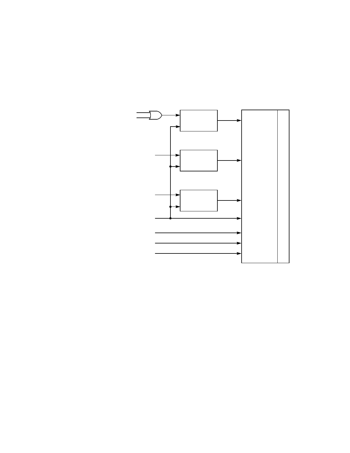
provides an example of a Flash ROM
configuration.
Figure 2.4
Flash ROM Block Diagram
The LSI53C1030 implements a Flash signature recognition mechanism
to determine if the Flash contains a valid image. The Flash can be
present and not contain a valid image either before its initial
programming or during board testing. The first access to the Flash is a
16-byte burst read beginning at Flash address 0x000000. The
LSI53C1030 compares the values read to the Flash signature values that
provides. If the signature values match, the LSI53C1030
performs the instruction located at Flash address 0x000000. If the
signature values do not match, the LSI53C1030 records an error and
ignores the Flash instruction. The Flash signature does not include the
first three bytes of Flash memory as these bytes contain a branch offset
instruction.
D
Q
CK
Flash R
OM (512 K x 8)
MAD[7:0]
D[7:0]
A[21:16]
FLSHALE[1]/
D
Q
FLSHALE[0]/
CK
A[15:8]
FLSHALE[1]/
A[7:0]
FLSHALE[0]/
CE/
FLSHCE/
OE/
MOE/
WE/
BWE[0]/
Upper Address
Middle Address
Lower Address
D
Q
CK