Zcr circuit diagram for lsi53c1030 and lsi53c1010r, Zero channel raid 2-29 – Avago Technologies LSI53C1030 User Manual
Page 59
Zero Channel RAID
2-29
Version 2.2
Copyright © 2001, 2002, 2003 by LSI Logic Corporation. All rights reserved.
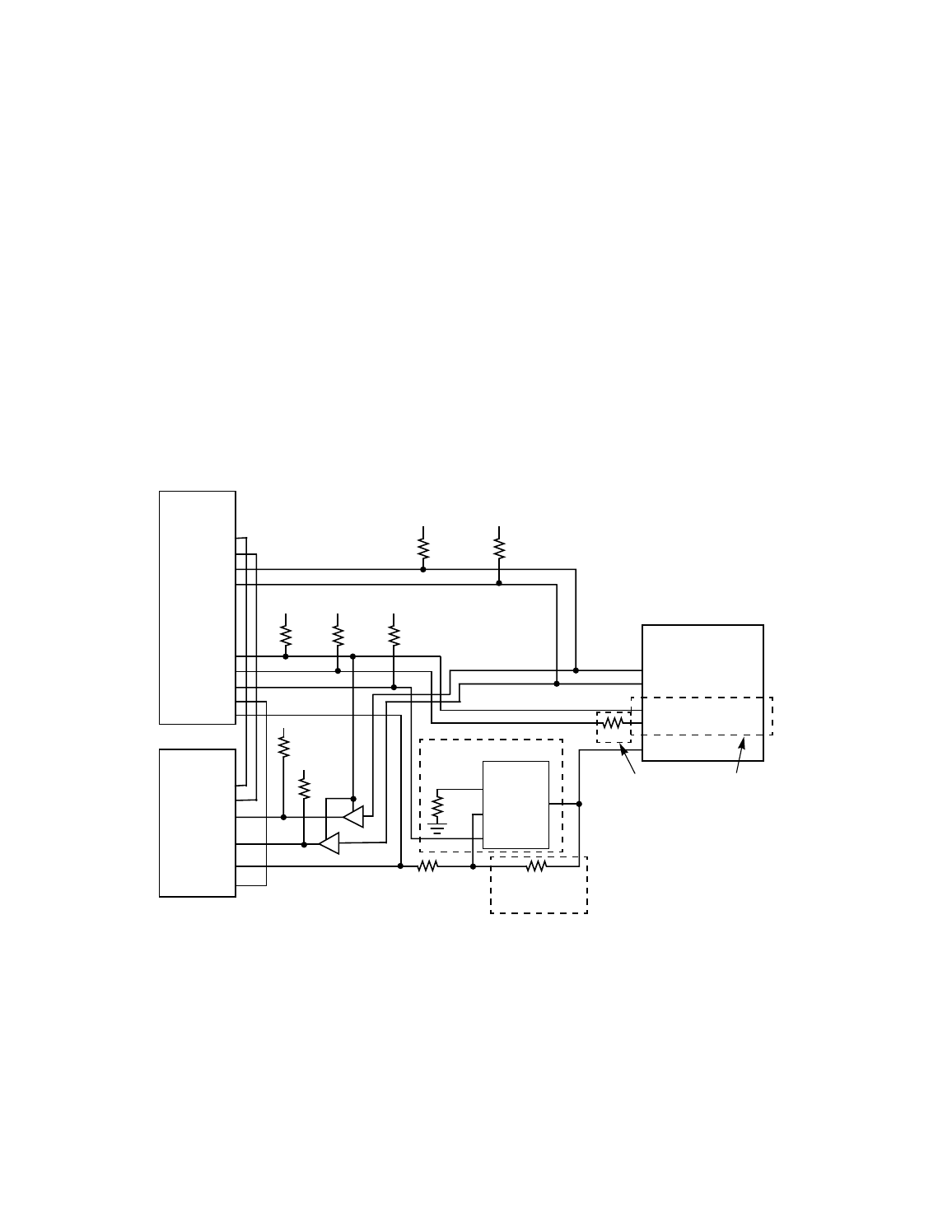
cycles to the LSI53C1030 when the I/O processor is granted the PCI bus.
This configuration also prevents the system processor from accessing
the LSI53C1030 PCI configuration registers.
LSI53C1030 based designs do not use the M66EN pin to determine the
PCI bus speed.
illustrates how to connect the LSI53C1030 to enable ZCR.
This figure also contains information for connecting the LSI53C1010R
based designs to a ZCR design and migrating from LSI53C1010R based
designs to LSI53C1030 based designs. Notice that the LSI53C1030 does
not require the 2:1 mux.
Figure 2.6
ZCR Circuit Diagram for LSI53C1030 and LSI53C1010R
ZCR PCI
Slot
LSI53C1010R/
Host System
IDSEL (AC13)
Int A/ (A6)
Int B/ (B7)
Int C/ (A7)
Int D/ (B8)
INTA/ (AC8)
INTB/ (AE7)
Int A/
Int B/
Int C/
Int D/
TDI (A4)
TMS (A3)
GNT/ (A17)
ZCR_EN/ (N23)
IOPD_ GNT/ (AC5)
No Pop for
2:1 Mux
No Pop for LSI53C1030
2:1 Mux
A0
A1
S0
B0
Vdd
Vdd
Vdd
LSI53C1030 Only
No Pop for
AD19
AD21
AD21 (B29)
IDSEL (A26)
4.7 k
Ω
Vdd
4.7 k
Ω
Vdd
4.7 k
Ω
Vdd
0.1 k
Ω
Vdd
0.1 k
Ω
0.1 k
Ω
0
Ω
0.1 k
Ω
Note: To maintain proper interrupt mapping, select the address line for use as IDSEL on the
LSI53C1010R/LSI53C1030 to be +2 address lines above IDSEL on ZCR slot.
0.1 k
Ω
0
Ω
LS53C1010R
LSI53C1010R
LSI53C1030
220
Ω