2 clock controller, Clock controller, Block diagram of clock controller – FUJITSU F2MC-8L F202RA User Manual
Page 70
54
CHAPTER 3 CPU
3.6.2
Clock Controller
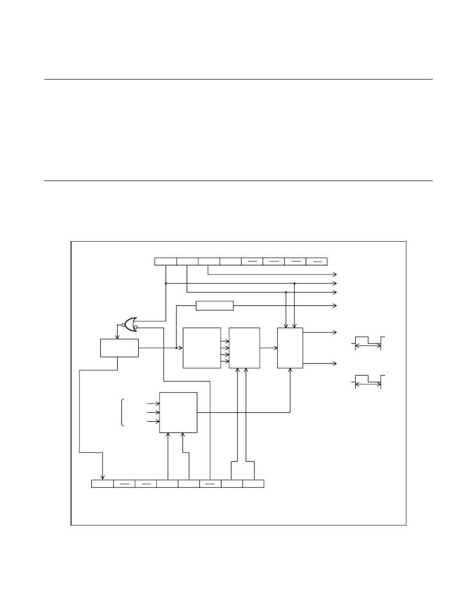
The clock controller consists of the following six blocks:
• Oscillation circuit
• System clock selector
• Clock controller
• Oscillation stabilization wait time selector
• System clock control register (SYCC)
• Standby control register (STBC)
■
Block Diagram of Clock Controller
Figure 3.6-4 is a block diagram of the clock controller.
Figure 3.6-4 Block Diagram of Clock Controller
S
TP
S
LP
S
PL
R
S
T
S
CM
WT1
WT0
C
S
1
C
S
0
2
14
/F
CH
2
17
/FCH
2
1
8
/FCH
1t
IN
S
T
1t
IN
S
T
F
CH
t
IN
S
T
S
t
a
nd
b
y control regi
s
ter (
S
TBC)
Pin control
S
top
S
leep
Clock for time-
bas
e
timer
1/2 fre
qu
ency
Clock
gener
a
tor
S
y
s
tem clock
s
elector
Pre-
s
c
a
ler
1/4 fre
qu
ency
1/
8
fre
qu
ency
1/16 fre
qu
ency
1/64 fre
qu
ency
S
elector
Clock
control
circ
u
it
Su
pplied to the CPU
Su
pplied to peripher
a
l
circ
u
it
s
From the
time-
bas
e
timer
O
s
cill
a
tion
s
t
ab
iliz
a
tion
w
a
it time
s
elector
S
y
s
tem clock control regi
s
ter (
S
YCC)
: O
s
cill
a
tion fre
qu
ency
: In
s
tr
u
ction cycle