FUJITSU F2MC-8L F202RA User Manual
Page 228
212
CHAPTER 9 12-BIT PPG TIMER
■
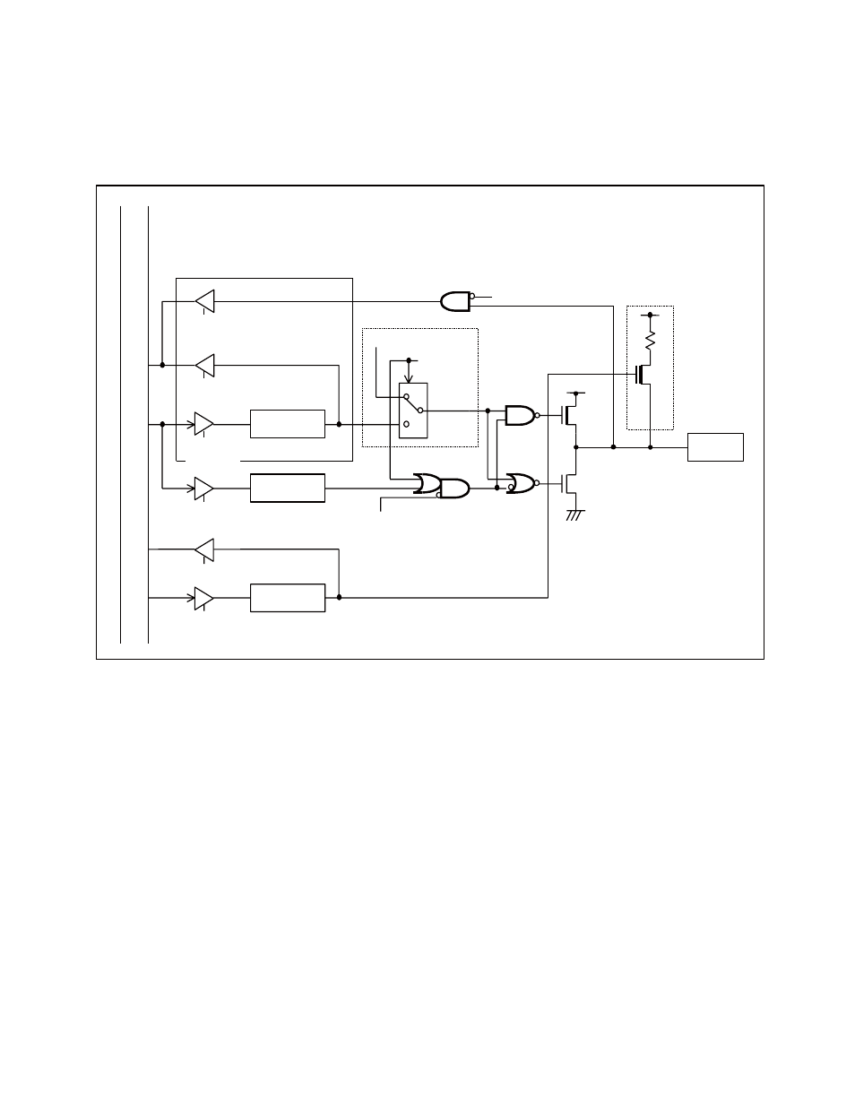
Block Diagram of Circuitry Terminating at the Pin Associated with the 12-bit PPG
Timer
Figure 9.3-1 Block Diagram of Circuitry Terminating at the P37/BZ/PPG Pin
Notes:
• If the ON setting of the pull-up resistor is selected by the pull-up setting register, the pin state will be
the "H" level (pull-up state) in stop mode (SPL = 1).
• Because buzzer outputs to the P37/BZ/PPG pin precede 12-bit PPG outputs to this pin, if the pin is
used as the PPG pin, turn the buzzer outputs off and set the RCEN bit such that PPG outputs are
enabled.
DDR
P-ch
N-ch
PDR
PUL
P37/BZ/PPG
Inter
nal data b
u
s
PDR read
PDR read
(when read-modify-write is
performed)
Output latch
PDR write
DDR write
PUL read
PUL write
Output from
peripheral
Output
enabl
from
peripheral
Stop mode (SPL = 1)
Pull-up resistor
Pin
Stop mode (SPL = 1)