Block diagram of port 4, Registers of port 4 – FUJITSU F2MC-8L F202RA User Manual
Page 107
91
CHAPTER 4 I/O PORTS
■
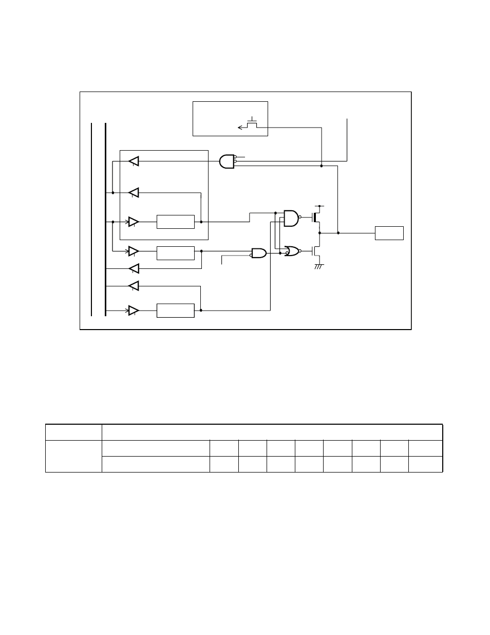
Block Diagram of Port 4
Figure 4.4-1 Block Diagram of Port 4
■
Registers of Port 4
The registers PDR4, DDR4, and OUT4 are associated with port 4.
The bits of these registers correspond to the pins of port 4 in one-to-one correspondence.
Table 4.4-2 tabulates the correspondence between the pins and the bits of the port 4 registers.
DDR
Pch
Nch
PDR
OUT
Inter
n
a
l d
a
t
a
bu
s
PDR re
a
d
PDR re
a
d
(when re
a
d-modify-write i
s
performed)
O
u
tp
u
t l
a
tch
PDR write
DDR write
S
top mode
(
S
PL = 1)
OUT re
a
d
OUT write
A/D converter
ch
a
nnel
s
elect
To A/D
converter'
s
a
n
a
log inp
u
t
A/D converter en
ab
le
b
it
Pin
s
S
top mode (
S
PL = 1)
DDR re
a
d
Table 4.4-2 Correspondence between the Pins and the Bits of the Port 4 Register
Port name
Bits of associated registers and corresponding pins
Port 4
PDR4, DDR4, OUT4
bit7
bit6
bit5
bit4
bit3
bit2
bit1
bit0
Pin corresponding to bit
-
-
-
-
P43
P42
P41
P40