Block diagram for 8-bit serial i/o pins – FUJITSU F2MC-8L F202RA User Manual
Page 334
318
CHAPTER 14 8-BIT SERIAL I/O
■
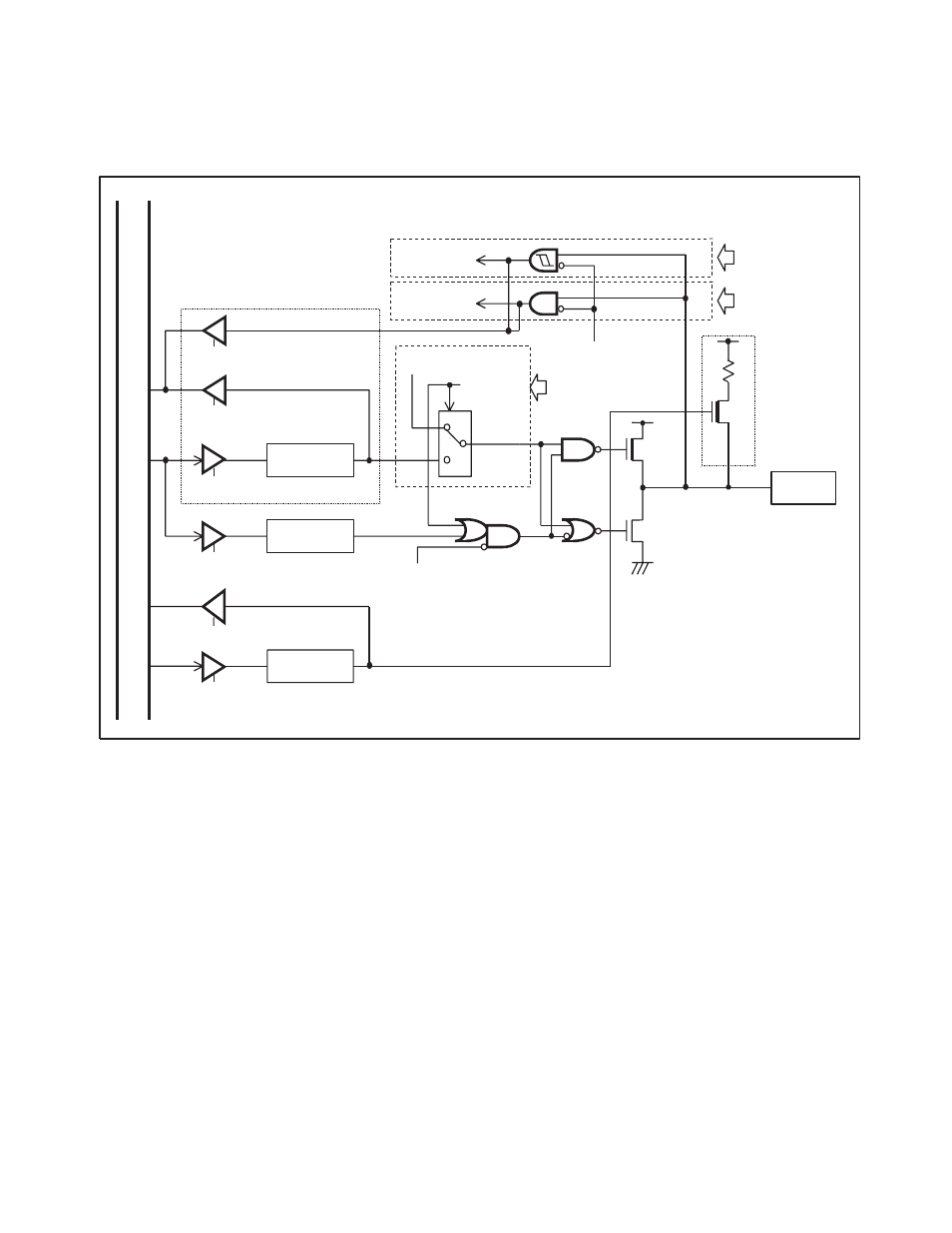
Block Diagram for 8-bit Serial I/O Pins
Figure 14.3-1 Block Diagram for 8-bit Serial I/O Pins
Note:
When "pull-up resistor available" is selected in the pull-up setting register, the pin state in stop mode
(SPL = 1) becomes high (pull-up state), not Hi-Z. During the reset, however, pull-up becomes invalid
and the pin state becomes Hi-Z.
DDR
Pch
Nch
S
CK
PDR
PUL
P
3
0/UCK/
S
CK
P
3
2/UI/
S
I
S
I
P
3
0/UCK/
S
CK
P
3
1/UO/
S
O
P
3
2/UI/
S
I
(
S
PL=1)
Inter
n
a
l d
a
t
a
bu
s
PDR re
a
d
Re
s
o
u
rce o
u
tp
u
t
S
top mode (
S
PL = 1)
Re
s
o
u
rce
o
u
tp
u
t
en
ab
le
Re
s
o
u
rce
o
u
tp
u
t
a
v
a
il
ab
le
P
u
ll-
u
p re
s
i
s
tor
PDR re
a
d
(At re
a
d-modify-write)
O
u
tp
u
t l
a
tch
PDR write
Pin
PUL re
a
d
PUL write
DDR write
S
top mode
This manual is related to the following products: