Figure 17.5-1 sho, Figure 17.5-1 i – FUJITSU F2MC-8L F202RA User Manual
Page 386
370
CHAPTER 17 FLASH MEMORY
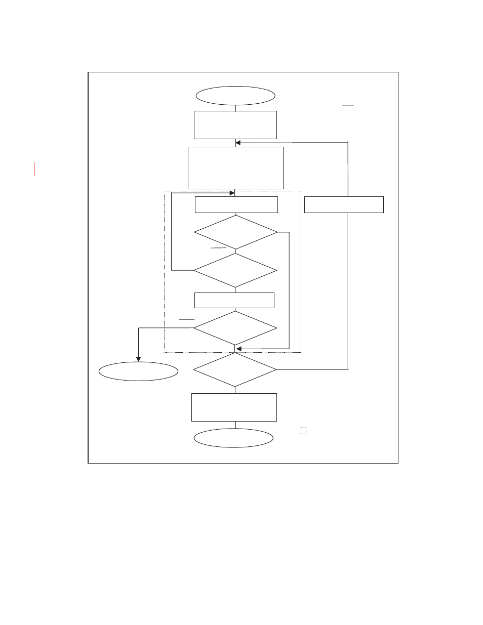
Figure 17.5-1 Example of the Flash Memory Write Procedure
D
a
t
a
D
a
t
a
D
a
t
a
0
1
D
a
t
a
S
t
a
rt writing*
M
a
ke
su
re +10V DC volt
a
ge
i
s
a
pplied
a
t the R
S
T pin
b
efore
s
t
a
rt writing
*
FMC
S
: WE (
b
it5)
En
ab
le fl
as
h memory write
Write comm
a
nd
s
e
qu
ence
(1) FAAA <-- AA
(2) F554 <-- 55
(
3
) FAAA <-- A0
(4) Write
a
ddre
ss
<-- Write d
a
t
a
Re
a
d intern
a
l
a
ddre
ss
Next
a
ddre
ss
D
a
t
a
polling (DQ7)
Timing limit (DQ5)
Re
a
d intern
a
l
a
ddre
ss
D
a
t
a
polling (DQ7)
Write error
Fin
a
l
a
ddre
ss
NO
YE
S
FMC
S
: WE (
b
it5)
Write-di
sab
le fl
as
h memory.
Complete writing
Confirm with the h
a
rdw
a
re
s
e
qu
ence fl
a
g
s
.
This manual is related to the following products:
See also other documents in the category FUJITSU Hardware:
- XG Series P3NK-4452-01ENZD (614 pages)
- FPCAC14C (1 page)
- MCJ3230SS (161 pages)
- MBA3073NC (138 pages)
- T5140 (102 pages)
- T5140 (76 pages)
- MAM3367MC/MP (152 pages)
- MPC3045AH (185 pages)
- MB2142-02 (23 pages)
- MB15F86UL (6 pages)
- MHS2030AT (40 pages)
- MHW2100BS (296 pages)
- MHK2060AT (227 pages)
- Disk Drives MHK2060AT (227 pages)
- MCM3064SS (170 pages)
- Mainboard D1561 (45 pages)
- MHC2040AT (219 pages)
- D1961 (45 pages)
- DISK DRIVES MHM2100AT (231 pages)
- MHR2010AT (250 pages)
- MHZ2120BJ (320 pages)
- MCE3064AP (175 pages)
- LQFP-64P (16 pages)
- Solaris PCI GigabitEthernet 3.0 (115 pages)
- MAY2036RC (94 pages)
- MAB3091 (142 pages)
- MPE3XXXAT (191 pages)
- MHV2040AH (40 pages)
- MHW2040AC (278 pages)
- ETERNUSmgr P2X0-0202-01EN (64 pages)
- VSS Hardware Provider 2.1 (134 pages)
- MAG3182FC (61 pages)
- MAU3147NC/NP (130 pages)
- MAX3147RC (94 pages)
- MHV2160BT (296 pages)
- MHV2040AT (280 pages)
- MAW3300NC/NP (130 pages)
- DeskPower E623 (50 pages)
- MAG3182LC (133 pages)
- OPTICAL DISK DRIVES MDG3064UB (42 pages)
- MHF2021AT (225 pages)
- MHR2040AT (40 pages)
- Single Drive FTM7926FB (1 page)
- PG-FCS103 (98 pages)
- MAS3735FC (114 pages)