FUJITSU F2MC-8L F202RA User Manual
Page 395
379
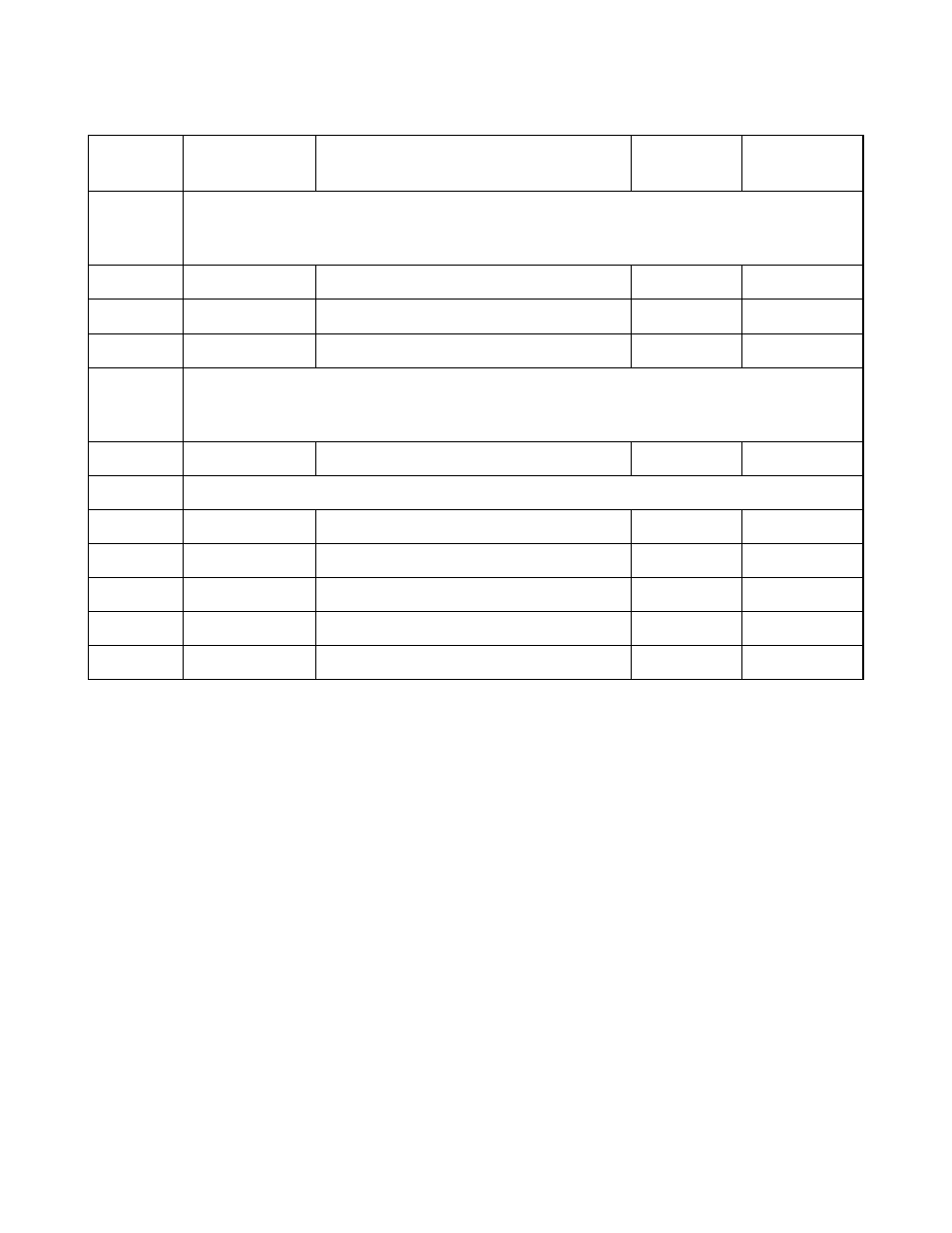
●
Explanation on read/write
R/W: Readable and Writable
R: Read only
W: Write only
●
Explanation on initial value
0: The initial value of this bit is "0".
1: The initial value of this bit is "1".
X: The initial value of this bit is undefined.
*: No used in MB89F202/F202RA.
Note:
Do not use the prohibited areas.
0066
H
to
006F
H
Vacancy
0070
H
PUL0
Port 0 pull-up set register
R/W
00000000
0071
H
PUL3
Port 3 pull-up set register
R/W
00000000
0072
H
PUL5
Port 5 pull-up set register
R/W
-------0
0073
H
to
0078
H
Prohibited area
0079
H
FMCS
Flash memory control status register
R/W, R
000X----
007A
H
Prohibited area
007B
H
ILR1
Interrupt level set register 1
W
11111111
007C
H
ILR2
Interrupt level set register 2
W
11111111
007D
H
ILR3
Interrupt level set register 3
W
11111111
007E
H
ILR4
Interrupt level set register 4
W
11111111
007F
H
ITR
Interrupt test register
Inhibited
------00
Table A-1 I/O Map (4 / 4)
Address
Register
abbreviation
Register name
Read/write
Initial value