Block diagram of port 7, Registers pdr7, ddr7, and pul7 of port 7 – FUJITSU F2MC-8L F202RA User Manual
Page 124
108
CHAPTER 4 I/O PORTS
■
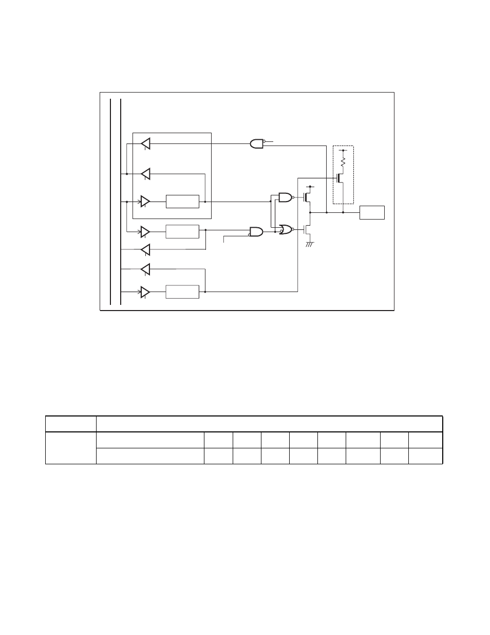
Block Diagram of Port 7
Figure 4.7-1 Block Diagram of Port 7
■
Registers PDR7, DDR7, and PUL7 of Port 7
Registers PDR7, DDR7, and PUL7 are associated with port 7.
The bits of these registers correspond to the pins of port 7 in one-to-one correspondence.
Table 4.7-2 tabulates the correspondence between the pins and the bits of the port 7 registers.
DDR
Pch
Nch
PDR
PUL
Inter
n
a
l d
a
t
a
bu
s
PDR re
a
d
PDR re
a
d
(when re
a
d-modify-write i
s
performed)
O
u
tp
u
t l
a
tch
PDR write
DDR write
PUL re
a
d
S
top mode (
S
PL = 1)
P
u
ll-
u
p re
s
i
s
tor
Pin
S
top mode (
S
PL = 1)
PUL write
DDR re
a
d
Table 4.7-2 Correspondence between the Pins and the Bits of the Port 7 Registers
Port name
Bits of associated registers and corresponding pins
Port 7
PDR7, DDR7, PUL7
bit7
bit6
bit5
bit4
bit3
bit2
bit1
bit0
Pin corresponding to bit
-
-
-
-
-
P72
P71
P70