FUJITSU F2MC-8L F202RA User Manual
Page 68
52
CHAPTER 3 CPU
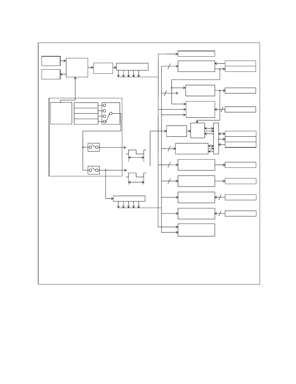
Figure 3.6-1 Clock Supply Map
F
CH
: O
s
cill
a
tion fre
qu
ency
t
IN
S
T
*1
*2
*
3
*4
UART
7
1t
IN
S
T
4
1t
IN
S
T
3
8
8
(*2)
(*1)
(*2)
(*2)
(*2)
(*1)
(*2)
X0 pin
O
s
cill
a
tion
circ
u
it
F
CH
1/2
fre
qu
ency
Time-
bas
e timer
S
top mode
O
s
cill
a
tion
control
1/4 fre
qu
ency
1/
8
fre
qu
ency
1/16 fre
qu
ency
1/64 fre
qu
ency
Clock controller
Ge
a
r
s
S
leep,
s
top, o
s
cill
a
tion
s
t
ab
iliz
a
tion w
a
it
S
top
Su
pplied to
CPU
Su
pplied to
peripher
a
l circ
u
it
s
Free-r
u
n co
u
nter
W
a
tchdog timer
8
/16-
b
it c
a
pt
u
re
timer/co
u
nter
EC pin
T0 pin
8
-
b
it PWM timer
PWM pin
(*2)
3
4
(*1)
(*2)
(*2)
(*4)
A/D converter
AN pin
Contin
u
o
us
conver
s
ion
Contin
u
o
us
conver
s
ion
Conver
s
ion/
comp
a
ri
s
on
UART
pre
s
c
a
ler
S
er
i
a
l
s
witch
UCK/
S
CK pin
U0/
S
0 pin
UI/
S
I pin
8
-
b
it
s
eri
a
l I/O
B
u
zzer
BZ pin
12-
b
it PPG
PPG pin
Extern
a
l interr
u
pt 1
INT1 pin
Extern
a
l interr
u
pt 2
INT2 pin
O
s
cill
a
tion
s
t
ab
iliz
a
tion
w
a
it time
: In
s
tr
u
ction cycle
: Not
a
ffected
b
y the ge
a
r.
: The ge
a
r
a
ffect
s
the oper
a
ting
s
peed or other
s
etting
s
.
: The time-
bas
e timer
s
top
s
when the o
s
cill
a
tion fre
qu
ency clock h
a
lt
s
.
: O
u
tp
u
t of the time-
bas
e timer i
s
s
elect
ab
le when the A/D converter i
s
a
ctiv
a
ted contin
u
o
us
ly.
Other oper
a
tion
s
a
re
a
ffected
b
y the ge
a
r.
3
(*
3
)
X1 pin