FUJITSU F2MC-8L F202RA User Manual
Page 280
264
CHAPTER 12 A/D CONVERTER
■
Block Diagram of the Pins Related to the A/D Converter
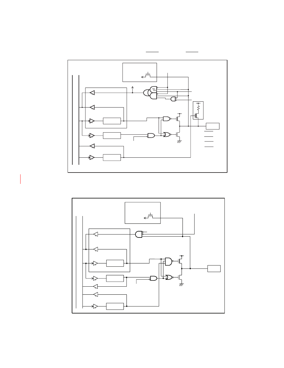
Figure 12.3-1 Block Diagram of P03/INT23/AN7 to P00/INT20/AN4 Pins
Figure 12.3-2 Block Diagram of P43/AN3 to P40/AN0 Pins
DDR
Pch
Nch
PDR
PUL
S
PL: Pin
s
t
a
t
us
s
etting
b
it of the
s
t
a
nd
b
y control regi
s
ter (
S
TBC)
A/D converter
ch
a
nnel
s
elect
A/D converter en
ab
le
b
it
(only P00 to P0
3
)
To the A/D
converter
a
n
a
log inp
u
t
To
a
n extern
a
l interr
u
pt
From di
sab
ling
a
n
extern
a
l interr
u
pt
PDR re
a
d
PDR re
a
d
S
top mode (
S
PL = 1)
(At re
a
d-modify-write)
P
u
ll-
u
p
re
s
i
s
tor
Inter
n
a
l d
a
t
a
bu
s
O
u
tp
u
t
l
a
tch
PDR write
DDR write
Pin
s
PUL re
a
d
PUL write
S
top mode (
S
PL = 1)
P00/INT20/AN4
P01/INT21/AN5
P02/INT22/AN6
P0
3
/INT2
3
/AN7
DDR
Pch
Nch
PDR
OUT
P40/AN0
P41/AN1
P42/AN2
P4
3
/AN
3
A/D converter
ch
a
nnel
s
elect
A/D converter
en
ab
le
b
it
To the A/D
converter
a
n
a
log inp
u
t
S
top mode (
S
PL = 1)
PDR re
a
d
Inter
n
a
l d
a
t
a
bu
s
PDR re
a
d
(At re
a
d-modify-write)
O
u
tp
u
t
l
a
tch
PDR write
Pin
s
DDR write
OUT re
a
d
OUT write
S
top mode
(
S
PL = 1)
DDR re
a
d