4 block diagram of mb89202/f202ra series, Block diagram of mb89202/f202ra series, 7chapter 1 overview – FUJITSU F2MC-8L F202RA User Manual
Page 23
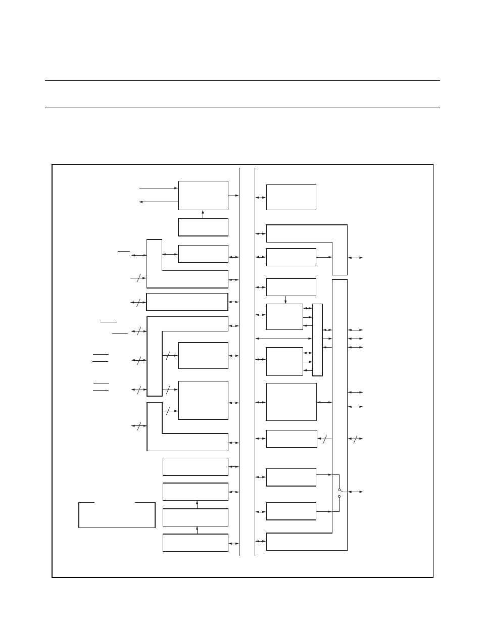
7
CHAPTER 1 OVERVIEW
1.4
Block Diagram of MB89202/F202RA Series
Figure 1.4-1 shows the block diagram of the MB89202/F202RA series.
■
Block Diagram of MB89202/F202RA Series
Figure 1.4-1 Block Diagram of MB89202/F202RA Series
X0
X1
R
S
T
P04 / INT24
to
P07 / INT27
P00 / INT20 / AN4,
P01 / INT21 / AN5
*
1
P40 / AN0
to
*
1
P4
3
/ AN
3
F
2
MC -
8
L CPU
Wild regi
s
ter
16K or
8
K
b
yte
s
ROM
512 or 256
b
yte
s
RAM
CMO
S
I/O port
(N-ch OD)
10-
b
it A/D
converter
Extern
a
l
interr
u
pt2
(w
a
ke-
u
p)
CMO
S
I/O port
Re
s
et circ
u
it
Clock controller
M
a
in clock
o
s
cill
a
tor
P
o
rt
4
P
or
t 0
V
CC
, V
SS
, C
12-
b
it PPG
B
u
zzer o
u
tp
u
t
CMO
S
I/O port
Extern
a
l interr
u
pt1
8
/16-
b
it
c
a
pt
u
re timer/
co
u
nter
8
-
b
it
s
eri
a
l I/O
8
-
b
it PWM
CMO
S
I/O port
Time-
bas
e timer
UART
Inter
n
a
l
bu
s
Po
rt
5
Po
rt
3
S
er
i
a
l f
u
nction
s
witching
UART pre
s
c
a
ler
P
3
7 / BZ / PPG
P
3
5 / INT11
P
3
6 / INT12
P
3
4 / TO / INT10
P
33
/ EC
P
3
2 / UI /
S
I
P
3
1 / UO /
S
O
P
3
0 / UCK /
S
CK
P50 / PWM
4
3
2
P02 / INT22 / AN6,
P0
3
/ INT2
3
/ AN7
2
4
4
8
4
Other pin
s
CMO
S
I/O port
Po
rt
6
2
P60, P61
CMO
S
I/O port
Po
rt
7
3
*
1
P70
to
*
1
P72
*
1
: L
a
rge-c
u
rrent drive type
*
2
: Check
s
ection
"
3
.1 Memory
S
p
a
ce
"
*
2
*
2