Block diagram of port 6, 101 chapter 4 i/o ports, Figure 4.6-1 block diagram of port6 – FUJITSU F2MC-8L F202RA User Manual
Page 117
101
CHAPTER 4 I/O PORTS
■
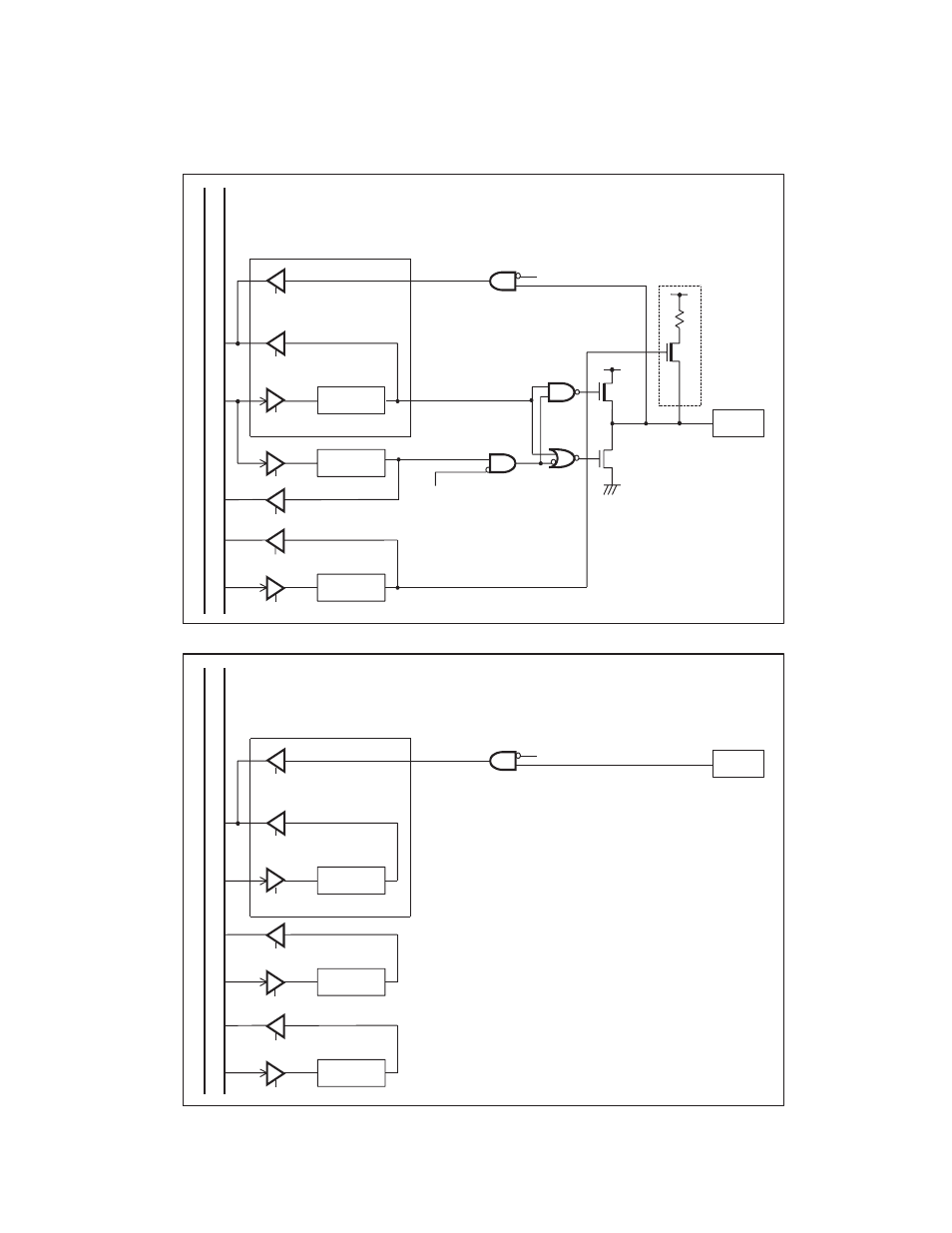
Block Diagram of Port 6
Figure 4.6-1 Block Diagram of Port6
DDR
P-ch
N-ch
PDR
PUL
Inter
n
a
l d
a
t
a
bu
s
PDR re
a
d
PDR re
a
d
(when re
a
d-modify-write i
s
performed)
O
u
tp
u
t l
a
tch
PDR write
DDR write
PUL re
a
d
S
top mode (
S
PL = 1)
P
u
ll-
u
p re
s
i
s
tor
Pin
S
top mode (
S
PL = 1)
PUL write
For MB
8
9202/V201
PDR
DDR
Inter
n
a
l d
a
t
a
bu
s
PDR re
a
d
PDR re
a
d
(when re
a
d-modify-write i
s
performed)
O
u
tp
u
t l
a
tch
PDR write
DDR re
a
d
Pin
S
top mode (
S
PL = 1)
DDR re
a
d
For MB
8
9F202/F202RA
PUL
PUL re
a
d
PUL write
DDR re
a
d
S
PL: Pin
s
t
a
te
s
etting
b
it of
s
t
a
nd
b
y control regi
s
ter (
S
TBC:
S
PL)
S
PL: Pin
s
t
a
te
s
etting
b
it of
s
t
a
nd
b
y control regi
s
ter (
S
TBC:
S
PL)
This manual is related to the following products: