Block diagram of port 3, Registers pdr3, ddr3, and pul3 of port 3 – FUJITSU F2MC-8L F202RA User Manual
Page 101
85
CHAPTER 4 I/O PORTS
■
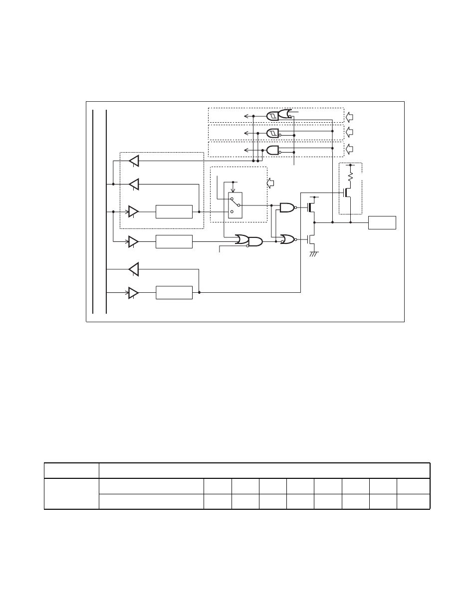
Block Diagram of Port 3
Figure 4.3-1 Block Diagram of Port 3
Note:
Because the value states of the pins are always input to the external interrupt circuit, when a pin is used
as a normal I/O port, the operation of the external interrupt circuit corresponding to the pin must be
inhibited. See "CHAPTER 10 EXTERNAL INTERRUPT CIRCUIT 1 (EDGE) ".
■
Registers PDR3, DDR3, and PUL3 of Port 3
The registers PDR3, DDR3, and PUL3 are associated with port 3.
The bits of these registers correspond to the pins of port 3 in one-to-one correspondence.
Table 4.3-2 tabulates the correspondence between the pins and the bits of port 3 registers.
DDR
Pch
Nch
PDR
PUL
Inter
n
a
l d
a
t
a
bu
s
PDR re
a
d
PDR write
PDR re
a
d
(when re
a
d-modify-write i
s
performed)
O
u
tp
u
t l
a
tch
DDR write
PUL re
a
d
PUL write
Extern
a
l
interr
u
pt
Inp
u
t to
peripher
a
l
Inp
u
t to
peripher
a
l
O
u
tp
u
t from peripher
a
l
O
u
tp
u
t
from
peripher
a
l
en
ab
le
S
top mode
(
S
PL = 1)
O
u
tp
u
t occ
u
rring
from peripher
a
l
Extern
a
l interr
u
pt
en
ab
le
Extern
a
l interr
u
pt
occ
u
rring
Hy
s
tere
s
i
s
inp
u
t
CMO
S
inp
u
t
P
u
ll-
u
p re
s
i
s
tor
Pin
s
S
top mode
(
S
PL = 1)
Table 4.3-2 Correspondence between the Pins and the Bits of Port 3 Registers
Port name
Bits of associated registers and corresponding pins
Port 3
PDR3, DDR3, PUL3
bit7
bit6
bit5
bit4
bit3
bit2
bit1
bit0
Pin corresponding to bit
P37
P36
P35
P34
P33
P32
P31
P30