Avago Technologies LSI53C895A User Manual
Page 333
Package Diagrams
6-73
LSI Logic component dimensions conform to a current revision of the
JEDEC Publication 95 standard package outline, using ANSI 14.5Y
“Dimensioning and Tolerancing” interpretations. As JEDEC drawings are
balloted and updated, changes may have occurred. To ensure the use of
a current drawing, the JEDEC drawing revision level should be verified.
Visit www.eia.org/jedec for review of Publication 95 drawings and revision
levels.
For printed circuit board land patterns that will accept LSI Logic
components, it is recommended that customers refer to the IPC
standards (Institute for Interconnecting and Packaging Electronic
Circuits). Specification number IPC-SM-782, Surface Mount Design and
Land Pattern Standard is an established method of designing land
patterns. Feature size and tolerances are industry standards based on
IPC assumptions.
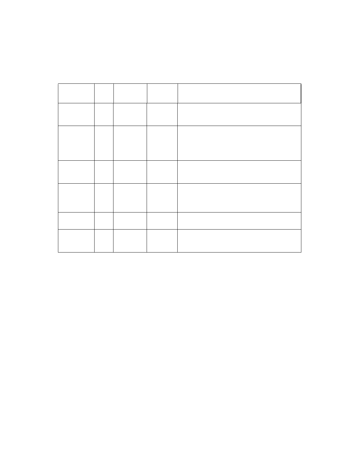
TEST_HSC/
I
82
J19
Previously TEST. TEST_HSC/ is used for
LSI Logic test purposes only. This signal can
cause a full chip reset.
V
DD
_RBIAS
RBIAS
I
129
130
A11
A10
Previously RBIAS
−
and RBIAS+. V
DD
_RBIAS and
RBIAS are functionally the same as RBIAS
−
and
RBIAS+ in the LSI53C895. They are used to
connect an external resistor to generate the bias
current used by LVDlink pads.
NC
N/A
4, 49
Y4, W18
Previously V5BIAS(P). It was used for voltage
biasing of the PCI signals. The biasing is now
automatically handled internally.
NC
N/A
62
T20
Previously V5BIAS(M). It was used for voltage
biasing of the external memory interface signals.
The biasing is now automatically handled
internally.
NC
N/A
177
J1
Previously TEST. It was never used in actual board
design.
NC
N/A
192
P3
Previously BIG_LIT/. It was used for big or little
endian selection, and is no longer used. The
LSI53C895A is little endian only.
Table 6.54
LSI53C895A vs. LSI53C895 Pin/Ball Differences (Cont.)
Pin/Ball
Name
Type
208 PQFP
Pin #
272 BGA
Ball #
Description