Table 6.17 interrupt output, Figure6.10 interrupt output, Pci and external memory interface timing diagrams – Avago Technologies LSI53C895A User Manual
Page 274: Interrupt output
6-14
Electrical Specifications
and
provide Interrupt Output timing data.
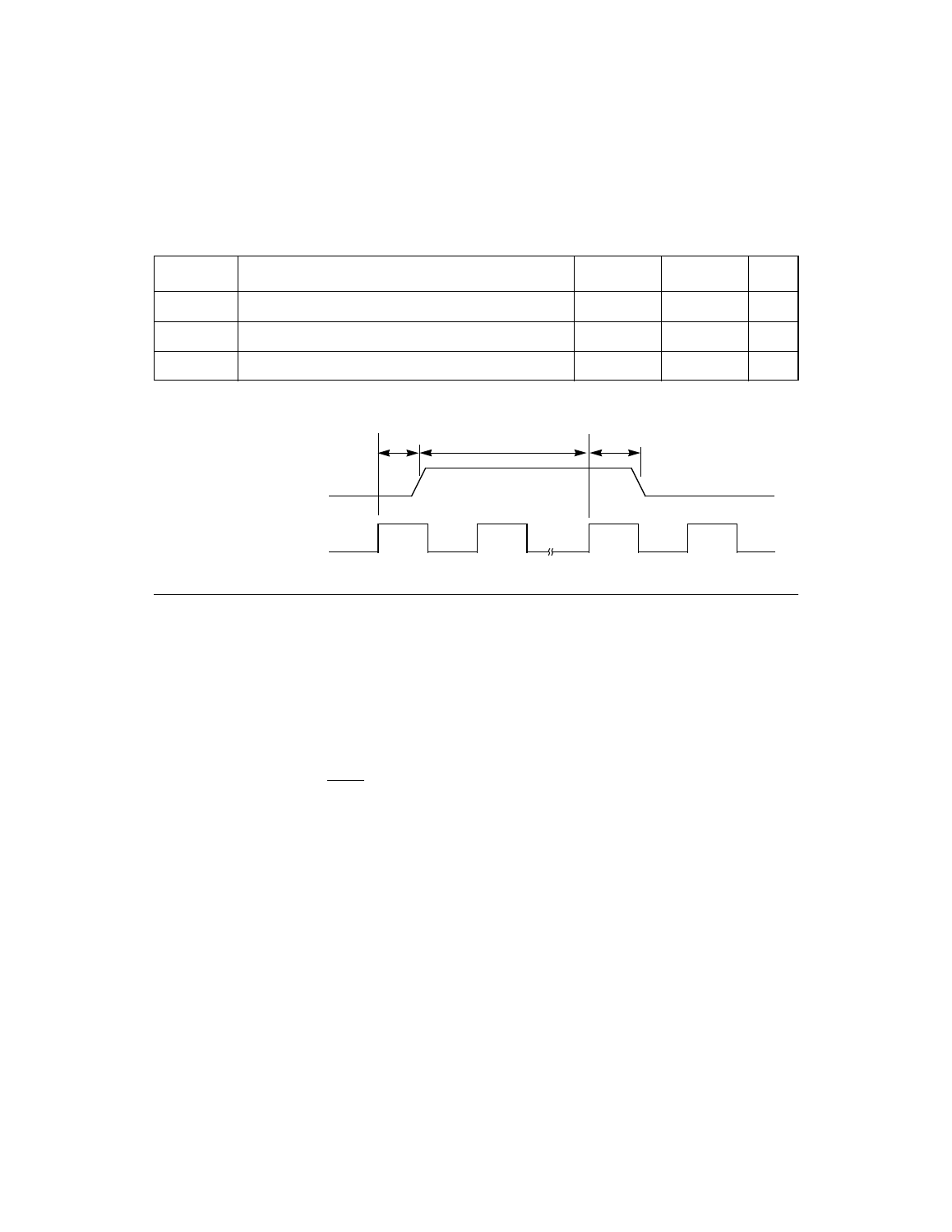
Figure 6.10 Interrupt Output
6.4 PCI and External Memory Interface Timing Diagrams
Figures
through
represent signal activity when the
LSI53C895A accesses the PCI bus. This section includes timing
diagrams for access to three groups of memory configurations. The first
group applies to
. The second group applies to
. The third group applies to
Note:
Multiple byte accesses to the external memory bus
increase the read or write cycle by 11 clocks for each
additional byte.
Timing diagrams included in this section are:
•
–
PCI Configuration Register Read
–
PCI Configuration Register Write
–
32-Bit Operating Register/SCRIPTS RAM Read
–
64-Bit Address Operating Register/SCRIPTS RAM Read
Table 6.17
Interrupt Output
Symbol
Parameter
Min
Max
Unit
t
1
CLK HIGH to IRQ/ LOW
2
11
ns
t
2
CLK HIGH to IRQ/ HIGH
2
11
ns
t
3
IRQ/ deassertion time
3
–
CLK
CLK
IRQ/
t
3
t
1
t
2