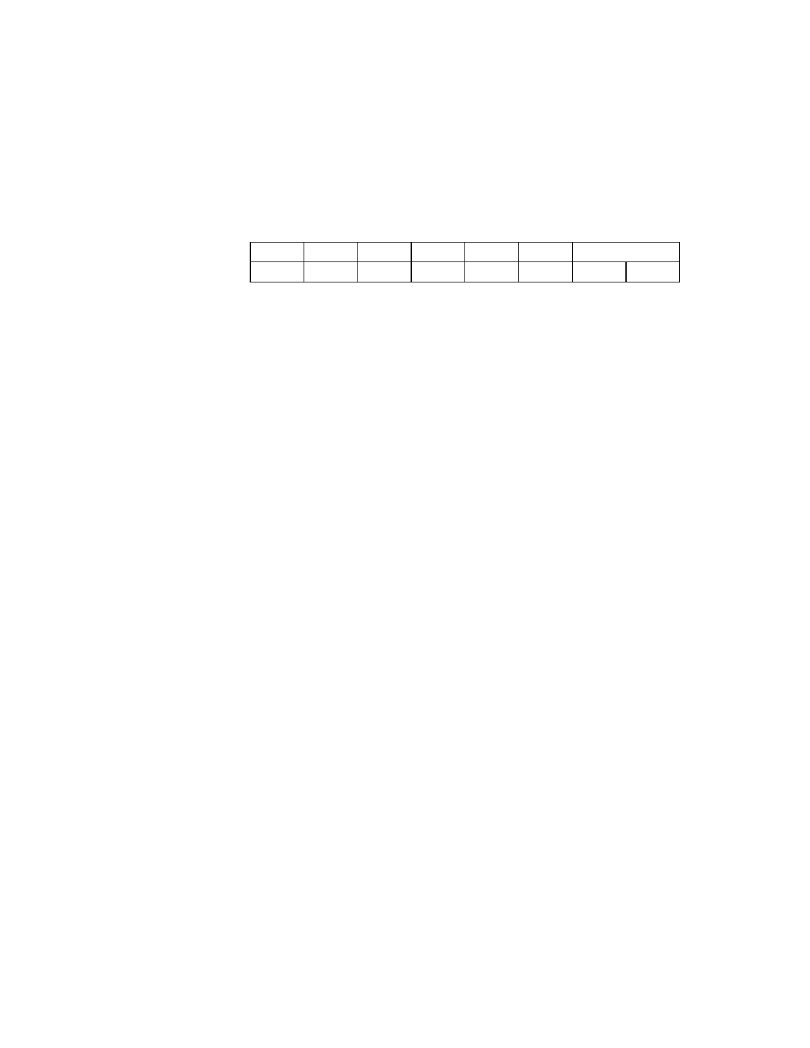
Chip test five (ctest5), Chip test, Five (ctest5) – Avago Technologies LSI53C895A User Manual
Page 170: Accessible). if b, That the i/o, Es the cost, Chip test five, Ctest5), Register: 0x22

4-62
Registers
Register: 0x22
Chip Test Five (CTEST5)
Read/Write
ADCK
Clock Address Incrementor
7
Setting this bit increments the address pointer contained
in the
register. The DNAD
register is incremented based on the DNAD contents and
the current DBC value. This bit automatically clears itself
after incrementing the DNAD register.
BBCK
Clock Byte Counter
6
Setting this bit decrements the byte count contained in
the 24-bit DBC register. It is decremented based on the
contents and the current
value. This bit automatically clears
itself after decrementing the DBC register.
DFS
DMA FIFO Size
5
This bit controls the size of the DMA FIFO. When clear,
the DMA FIFO appears as only 112 bytes deep. When
set, the DMA FIFO size increases to 944 bytes. Using an
112-byte FIFO allows software written for other
LSI53C8XX family chips to properly calculate the number
of bytes residing in the chip after a target disconnect. The
default value of this bit is zero.
MASR
Master Control for Set or Reset Pulses
4
This bit controls the operation of bit 3. When this bit is
set, bit 3 asserts the corresponding signals. When this bit
is cleared, bit 3 deasserts the corresponding signals. Do
not change this bit and bit 3 in the same write cycle.
DDIR
DMA Direction
3
Setting this bit either asserts or deasserts the internal
DMA Write (DMAWR) direction signal depending on the
current status of the MASR bit in this register. Asserting
the internal DMA write signal indicates that data is
7
6
5
4
3
2
1
0
ADCK
BBCK
DFS
MASR
DDIR
BL2
BO[9:8]
0
0
0
0
0
0
0
0
