Register: 0x57 – Avago Technologies LSI53C895A User Manual
Page 208

4-100
Registers
Register: 0x57
Chip Control 1 (CCNTL1)
Read/Write
ZMODE
High Impedance Mode
7
Setting this bit causes the LSI53C895A to place all output
and bidirectional pins except MAC/_TESTOUT, into a
high impedance state. Also, setting this bit causes all I/O
pins to become inputs, and all pull-ups and pull-downs to
be disabled. When this bit is set, the MAC/_TESTOUT
pin becomes the output pin for the connectivity test of the
LSI53C895A signals in the “AND-tree” test mode. In
order to read data out of the LSI53C895A, this bit must
be cleared. This bit is intended for board-level testing
only. Do not set this bit during normal system operation.
R
Reserved
[6:4]
DDAC
Disable Dual Address Cycle
3
When this bit is set, all 64-bit addressing as a master will
be disabled. No dual address cycles will be generated by
the LSI53C895A.
When this bit is cleared, the LSI53C895A will generate
dual address cycles based on the master operation being
performed and the value of its associated selector
register.
64TIMOD
64-Bit Table Indirect Indexing Mode
2
When this bit is cleared, bits [24:28] of the first table entry
Dword will select one of 22 possible selectors to be used
in a BMOV operation. When this bit is set, bits [24:31] of
the first table entry Dword will be copied directly into
DNAD64 to provide 40-bit addressing capability. This bit
will only function if the EN64TIBMV bit is set.
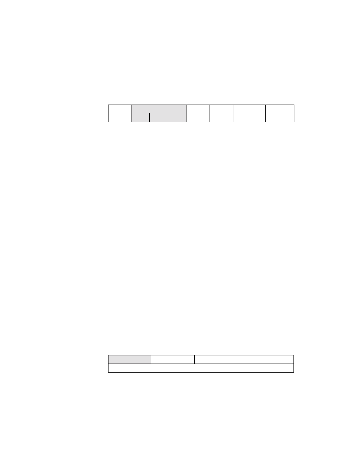
Index Mode 0 (64TIMOD clear) table entry format:
7
6
4
3
2
1
0
ZMODE
R
DDAC
64TIMOD
EN64TIBMV
EN64DBMV
0
x
x
x
0
0
0
0
[31:29]
[28:24]
[23:0]
Reserved
Sel Index
Byte Count
Source/Destination Address [31:0]
