Bit operating register/scripts ram write – Avago Technologies LSI53C895A User Manual
Page 280
6-20
Electrical Specifications
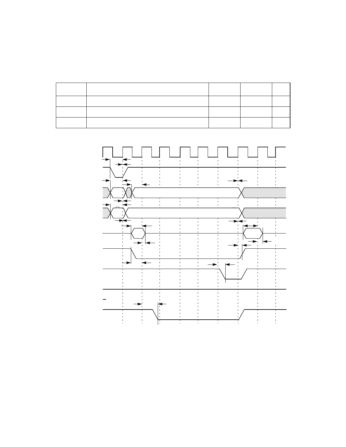
Figure 6.15 32-Bit Operating Register/SCRIPTS RAM Write
Table 6.22
32-Bit Operating Register/SCRIPTS RAM Write
Symbol
Parameter
Min
Max
Unit
t
1
Shared signal input setup time
7
–
ns
t
2
Shared signal input hold time
0
–
ns
t
3
CLK to shared signal output valid
–
11
ns
CLK
(Driven by System)
FRAME/
(Driven by Master)
AD
(Driven by Master)
C_BE/
(Driven by Master)
PAR
(Driven by Master)
IRDY/
(Driven by Master)
TRDY/
(Driven by LSI53C895A)
STOP/
(Driven by LSI53C895A)
DEVSEL/
(Driven by LSI53C895A)
Addr
In
CMD
In
t
3
In
t
1
t
1
t
1
t
1
t
1
t
1
t
2
t
2
t
2
t
2
t
2
t
2
t
1
t
3
t
2
t
2
See also other documents in the category Avago Technologies Hardware:
- MGA-725M4 (4 pages)
- MGA-71543 (4 pages)
- MGA-71543 (3 pages)
- MGA-82563 (6 pages)
- 3ware SAS 9750-8i (48 pages)
- 3ware 9690SA-8I (Channel) (138 pages)
- 3ware 9690SA-8I (Channel) (380 pages)
- 3ware SAS 9750-8i (29 pages)
- 3ware 9550SXU-8LP (Channel) (149 pages)
- 3ware 9550SXU-8LP (Channel) (40 pages)
- 3ware 9650SE-8LPML (Channel) (45 pages)
- 3ware 9690SA-8I (Channel) (361 pages)
- 3ware 9690SA-8I (Channel) (27 pages)
- 6160 SAS Switch (2 pages)
- MegaRAID SAS 9271-8iCC (13 pages)
- MegaRAID SAS 9361-8i (13 pages)
- MegaRAID SAS 9266-8i (12 pages)
- MegaRAID SAS 9380-8e (43 pages)
- Cache Protection for RAID Controller Cards (139 pages)
- Cache Protection for RAID Controller Cards (13 pages)
- MegaRAID SAS 9285-8ecv (80 pages)
- MegaRAID SAS 9285-8ecv (92 pages)
- MegaRAID SAS 9266-8i (20 pages)
- MegaRAID SAS 9271-8iCC (26 pages)
- MegaRAID SafeStore Software (502 pages)
- MegaRAID SAS 0260CV-4i (64 pages)
- MegaRAID SAS 0260CV-4i (49 pages)
- MegaRAID SAS 9271-8i (8 pages)
- MegaRAID SAS 0260CV-4i (72 pages)
- MegaRAID SAS 9361-8i (7 pages)
- MegaRAID SAS 9341-8i (8 pages)
- MegaRAID SAS 9380-4i4e (7 pages)
- MegaRAID SAS 9380-8e (7 pages)
- MegaRAID SAS 0260CV-4i (28 pages)
- MegaRAID SAS 9240-8i (4 pages)
- MegaRAID SAS 9260-16i (12 pages)
- MegaRAID SAS 9280-24i4e (14 pages)
- MegaRAID SAS 9280-24i4e (16 pages)
- MegaRAID SAS 9260-8i (4 pages)
- MegaRAID SafeStore Software (8 pages)
- MegaRAID SAS 9280-8e (22 pages)
- MegaRAID SAS 9261-8i (4 pages)
- MegaRAID SAS 9285-8e (12 pages)
- MegaRAID SAS 9280-16i4e (12 pages)
- MegaRAID SAS 9280-4i4e (4 pages)