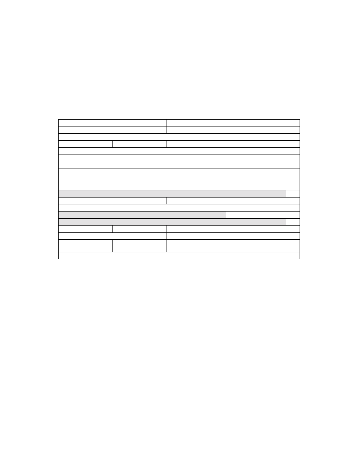
Table 4.1 pci configuration register map, Pci configuration register map, Table 4.1 – Avago Technologies LSI53C895A User Manual
Page 110
4-2
Registers
not supported are not writable and return all zeros when read. Only those
registers and bits that are currently supported by the LSI53C895A are
described in this chapter. Reserved bits should not be accessed
.
Table 4.1
PCI Configuration Register Map
31
16 15
0
0x00
0x04
Not Supported
Base Address Register Zero (I/O)
0x10
Base Address Register One (MEMORY)
bits [31:0]
0x14
Base Address Register Two (SCRIPTS RAM)
0x18
Not Supported
0x1C
Not Supported
0x20
Not Supported
0x24
Reserved
0x28
0x2C
0x30
Reserved
Reserved
0x38
Power Management Capabilities (PMC)
Power Management Control/Status (PMCSR)
0x44
0x48
See also other documents in the category Avago Technologies Hardware:
- MGA-725M4 (4 pages)
- MGA-71543 (4 pages)
- MGA-71543 (3 pages)
- MGA-82563 (6 pages)
- 3ware SAS 9750-8i (48 pages)
- 3ware 9690SA-8I (Channel) (138 pages)
- 3ware 9690SA-8I (Channel) (380 pages)
- 3ware SAS 9750-8i (29 pages)
- 3ware 9550SXU-8LP (Channel) (149 pages)
- 3ware 9550SXU-8LP (Channel) (40 pages)
- 3ware 9650SE-8LPML (Channel) (45 pages)
- 3ware 9690SA-8I (Channel) (27 pages)
- 3ware 9690SA-8I (Channel) (361 pages)
- 6160 SAS Switch (2 pages)
- MegaRAID SAS 9266-8i (12 pages)
- MegaRAID SAS 9380-8e (43 pages)
- Cache Protection for RAID Controller Cards (139 pages)
- Cache Protection for RAID Controller Cards (13 pages)
- MegaRAID SAS 9271-8iCC (13 pages)
- MegaRAID SAS 9361-8i (13 pages)
- MegaRAID SAS 9266-8i (20 pages)
- MegaRAID SAS 9271-8iCC (26 pages)
- MegaRAID SafeStore Software (502 pages)
- MegaRAID SAS 9285-8ecv (80 pages)
- MegaRAID SAS 9285-8ecv (92 pages)
- MegaRAID SAS 0260CV-4i (64 pages)
- MegaRAID SAS 0260CV-4i (49 pages)
- MegaRAID SAS 9271-8i (8 pages)
- MegaRAID SAS 0260CV-4i (72 pages)
- MegaRAID SAS 9361-8i (7 pages)
- MegaRAID SAS 9341-8i (8 pages)
- MegaRAID SAS 9380-4i4e (7 pages)
- MegaRAID SAS 9380-8e (7 pages)
- MegaRAID SAS 0260CV-4i (28 pages)
- MegaRAID SAS 9240-8i (4 pages)
- MegaRAID SAS 9260-16i (12 pages)
- MegaRAID SAS 9280-24i4e (14 pages)
- MegaRAID SAS 9280-24i4e (16 pages)
- MegaRAID SAS 9260-8i (4 pages)
- MegaRAID SafeStore Software (8 pages)
- MegaRAID SAS 9280-8e (22 pages)
- MegaRAID SAS 9261-8i (4 pages)
- MegaRAID SAS 9285-8e (12 pages)
- MegaRAID SAS 9280-16i4e (12 pages)
- MegaRAID SAS 9280-4i4e (4 pages)