Avago Technologies LSI53C895A User Manual
Page 169
SCSI Registers
4-61
LSI53C895A is informed of the error by the PERR/ pin
being asserted by the target. When this bit is cleared, the
LSI53C895A does not interrupt if a master parity error
occurs. This bit is cleared at power-up.
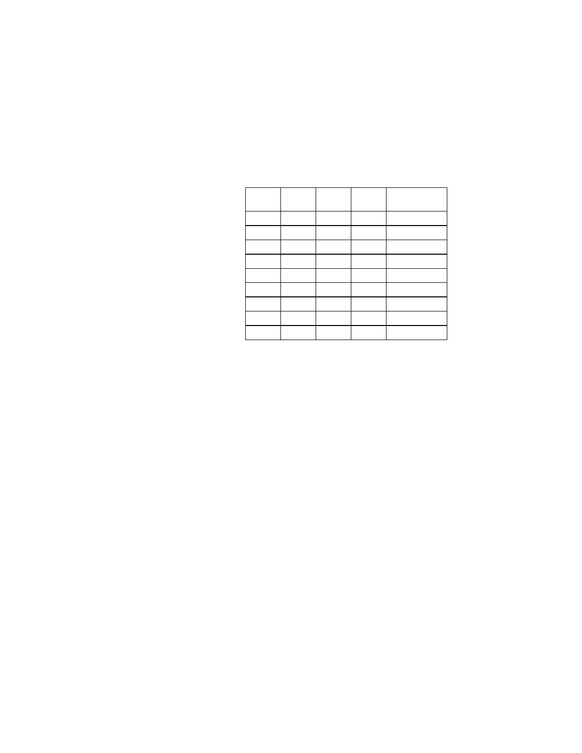
FBL[2:0]
FIFO Byte Control
[2:0]
These bits steer the contents of the
register to the appropriate byte lane of the
64-bit DMA FIFO. If the FBL3 bit is set, then FBL2
through FBL0 determine which of eight byte lanes can be
read or written. When cleared, the byte lane read or
written is determined by the current contents of the
and
registers. Each of the eight bytes that make up the 64-bit
DMA FIFO is accessed by writing these bits to the proper
value. For normal operation, FBL3 must equal zero.
FBL3
FBL2
FBL1
FBL0
DMA FIFO
Byte Lane
0
x
x
x
Disabled
1
0
0
0
0
1
0
0
1
1
1
0
1
0
2
1
0
1
1
3
1
1
0
0
4
1
1
0
1
5
1
1
1
0
6
1
1
1
1
7
- MGA-725M4 (4 pages)
- MGA-71543 (4 pages)
- MGA-71543 (3 pages)
- MGA-82563 (6 pages)
- 3ware SAS 9750-8i (48 pages)
- 3ware 9690SA-8I (Channel) (138 pages)
- 3ware 9690SA-8I (Channel) (380 pages)
- 3ware SAS 9750-8i (29 pages)
- 3ware 9550SXU-8LP (Channel) (149 pages)
- 3ware 9550SXU-8LP (Channel) (40 pages)
- 3ware 9650SE-8LPML (Channel) (45 pages)
- 3ware 9690SA-8I (Channel) (27 pages)
- 3ware 9690SA-8I (Channel) (361 pages)
- 6160 SAS Switch (2 pages)
- MegaRAID SAS 9266-8i (12 pages)
- MegaRAID SAS 9380-8e (43 pages)
- Cache Protection for RAID Controller Cards (139 pages)
- Cache Protection for RAID Controller Cards (13 pages)
- MegaRAID SAS 9271-8iCC (13 pages)
- MegaRAID SAS 9361-8i (13 pages)
- MegaRAID SAS 9266-8i (20 pages)
- MegaRAID SAS 9271-8iCC (26 pages)
- MegaRAID SafeStore Software (502 pages)
- MegaRAID SAS 9285-8ecv (80 pages)
- MegaRAID SAS 9285-8ecv (92 pages)
- MegaRAID SAS 0260CV-4i (64 pages)
- MegaRAID SAS 0260CV-4i (49 pages)
- MegaRAID SAS 9271-8i (8 pages)
- MegaRAID SAS 0260CV-4i (72 pages)
- MegaRAID SAS 9361-8i (7 pages)
- MegaRAID SAS 9341-8i (8 pages)
- MegaRAID SAS 9380-4i4e (7 pages)
- MegaRAID SAS 9380-8e (7 pages)
- MegaRAID SAS 0260CV-4i (28 pages)
- MegaRAID SAS 9240-8i (4 pages)
- MegaRAID SAS 9260-16i (12 pages)
- MegaRAID SAS 9280-24i4e (14 pages)
- MegaRAID SAS 9280-24i4e (16 pages)
- MegaRAID SAS 9260-8i (4 pages)
- MegaRAID SafeStore Software (8 pages)
- MegaRAID SAS 9280-8e (22 pages)
- MegaRAID SAS 9261-8i (4 pages)
- MegaRAID SAS 9285-8e (12 pages)
- MegaRAID SAS 9280-16i4e (12 pages)
- MegaRAID SAS 9280-4i4e (4 pages)