Scsi output data latch (sodl), Scsi output data latch, Sodl) – Avago Technologies LSI53C895A User Manual
Page 205: Scsi output, Data latch (sodl), Caution, Writing to, Reloaded at the beginning of a, Get receives, Enhancement, bit 1
SCSI Registers
4-97
LOCK
Frequency Lock
5
This bit is used when enabling the SCSI clock quadrupler,
which allows the LSI53C895A to transfer data at Ultra2
SCSI rates. Poll this bit for a 1 to determine that the clock
quadrupler has locked to 160 MHz. For more information
on enabling the clock quadrupler, refer to the descriptions
of
, bits 2 and 3.
R
Reserved
[4:0]
Register: 0x53
Reserved
Registers: 0x54–0x55
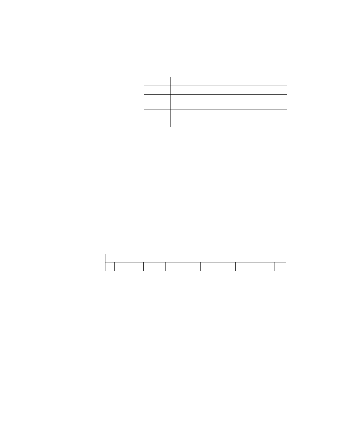
SCSI Output Data Latch (SODL)
Read/Write
SODL
SCSI Output Data Latch
[15:0]
This register is used primarily for diagnostic testing or
programmed I/O operation. Data written to this register is
asserted onto the SCSI data bus by setting the Assert
Data Bus bit in the
register.
This register is used to send data using programmed I/O.
Data flows through this register when sending data in any
mode. It is also used to write to the synchronous data
FIFO when testing the chip. The power-up value of this
register is indeterminate.
Bit [7:6]
Operating Mode
00
Not Possible
01
HVD or powered down
(for HVD mode, the
bit must also be set)
10
SE
11
LVD SCSI
15
0
SODL
x
x
x
x
x
x
x
x
x
x
x
x
x
x
x
x