Dma control (dcntl), Control (dcntl), Dma control – Avago Technologies LSI53C895A User Manual
Page 179: Dcntl), 0x3b, Register: 0x3a, Register: 0x3b
SCSI Registers
4-71
The IRQ/ output is latched. Once asserted, it will remain asserted until
the interrupt is cleared by reading the appropriate status register.
Masking an interrupt after the IRQ/ output is asserted does not cause
deassertion of IRQ/.
For more information on interrupts, see
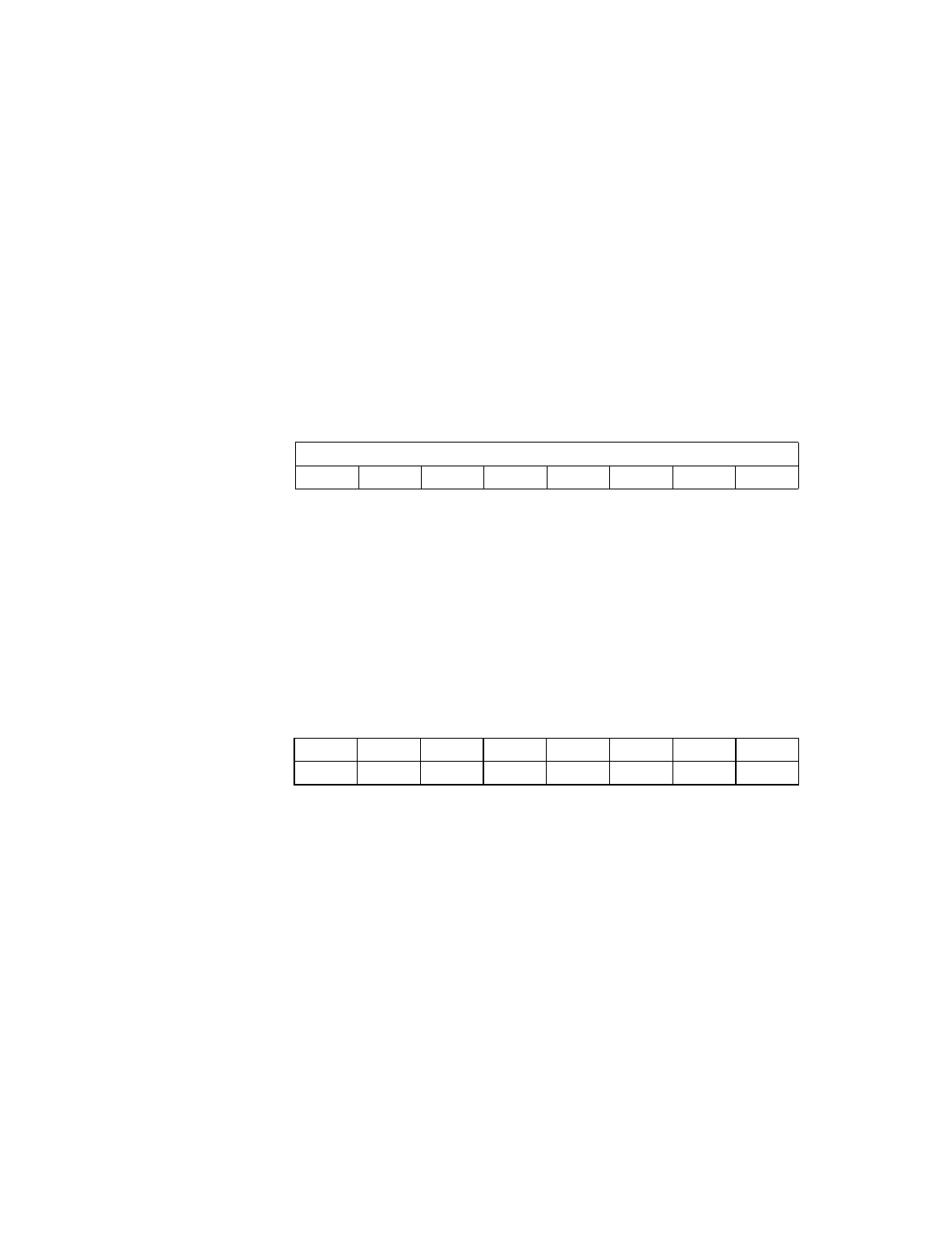
Register: 0x3A
Scratch Byte Register (SBR)
Read/Write
SBR
Scratch Byte Register
[7:0]
This is a general purpose register. Apart from CPU
access, only Register Read/Write and Memory Moves
into this register alter its contents. The default value of
this register is zero. This register is called the DMA
Watchdog Timer on previous LSI53C8XX family products.
Register: 0x3B
DMA Control (DCNTL)
Read/Write
CLSE
Cache Line Size Enable
7
Setting this bit enables the LSI53C895A to sense and
react to cache line boundaries set up by the
or PCI
register, whichever
contains the smaller value. Clearing this bit disables the
cache line size logic and the LSI53C895A monitors the
cache line size using the DMODE register.
PFF
Prefetch Flush
6
Setting this bit causes the prefetch unit to flush its
contents. The bit clears after the flush is complete.
7
0
SBR
0
0
0
0
0
0
0
0
7
6
5
4
3
2
1
0
CLSE
PFF
PFEN
SSM
IRQM
STD
IRQD
COM
0
0
0
0
0
0
0
0