Phase mismatch jump address 2 (pmjad2), Registers: 0xc4–0xc7, Registers: 0xc8–0xcb – Avago Technologies LSI53C895A User Manual
Page 217
Phase Mismatch Jump Registers
4-109
Registers: 0xC4–0xC7
Phase Mismatch Jump Address 2 (PMJAD2)
Read/Write
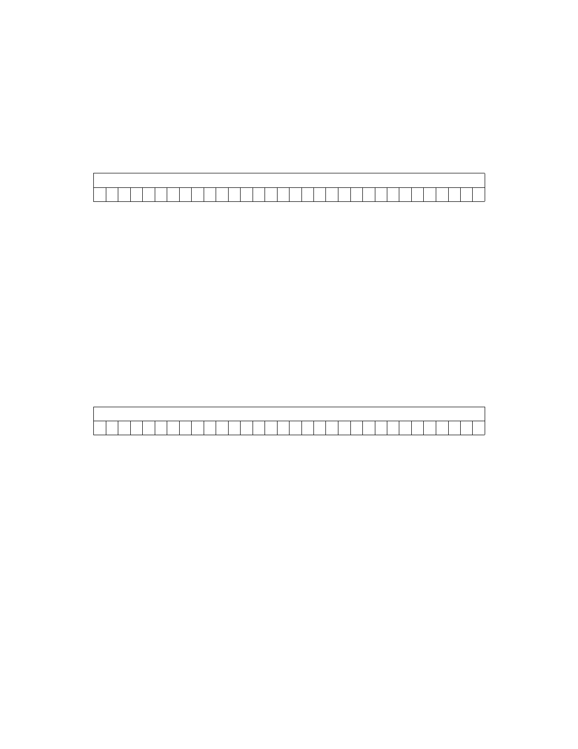
PMJAD2
Phase Mismatch Jump Address 2
[31:0]
This register contains the 32-bit address that will be
jumped to upon a phase mismatch. Depending upon the
state of the PMJCTL bit in register
this address will either be used during an
inbound (data in, status, message in) phase mismatch
(PMJCTL = 0) or when the WSR bit is set (PMJCTL = 1).
It should be loaded with an address of a SCRIPTS
routine that will handle the updating of memory data
structures of the BMOV that was executing when the
phase mismatch occurred.
Registers: 0xC8–0xCB
Remaining Byte Count (RBC)
Read/Write
RBC
Remaining Byte Count (RBC)
[31:0]
This register contains the byte count that remains for the
BMOV that was executing when the phase mismatch
occurred. In the case of direct or indirect BMOV
instructions, the upper byte of this register will also
contain the opcode of the BMOV that was executing. In
the case of a table indirect BMOV instruction, the upper
byte will contain the upper byte of the table indirect entry
that was fetched.
In the case of a SCSI data receive, this byte count will
reflect all data received from the SCSI bus, including any
byte in
. There will be no
data remaining in the part that must be flushed to
31
0
PMJAD2
0
0
0
0
0
0
0
0
0
0
0
0
0
0
0
0
0
0
0
0
0
0
0
0
0
0
0
0
0
0
0
0
31
0
RBC
0
0
0
0
0
0
0
0
0
0
0
0
0
0
0
0
0
0
0
0
0
0
0
0
0
0
0
0
0
0
0
0