Avago Technologies LSI53C895A User Manual
Page 103
Flash ROM and Memory Interface Signals
3-15
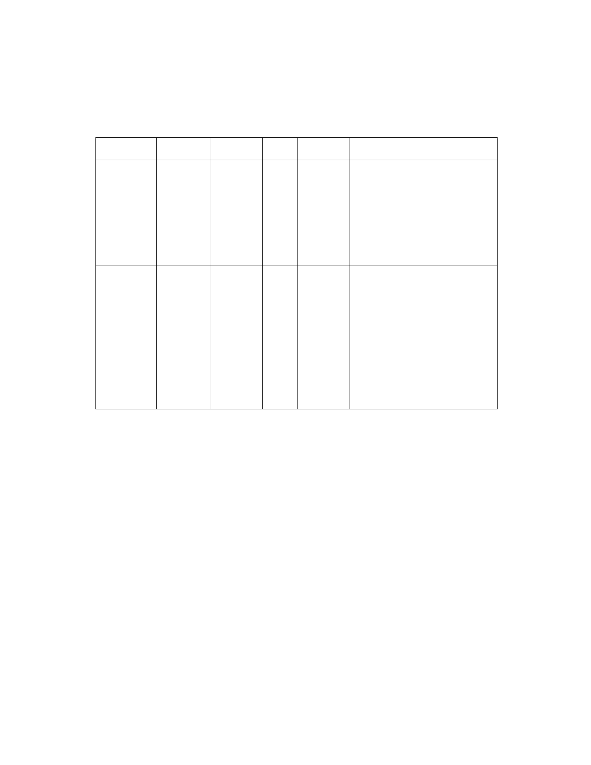
MAS1/
185
M1
O
4 mA
Memory Address Strobe 1. This
pin is used to latch in the most
significant address byte (bits [15:8])
of an external EEPROM or flash
memory. Since the LSI53C895A
moves addresses eight bits at a
time, this pin connects to the clock
of an external bank of flip-flops
which assemble up to a 20-bit
address for the external memory.
MAD[7:0]
69, 70, 71,
72, 74, 75,
76, 77
N19, N20,
M18, M19,
M20, L19,
L20, K20
I/O
4 mA
Memory Address/Data Bus. This
bus is used in conjunction with the
memory address strobe pins and
external address latches to
assemble up to a 20-bit address for
an external EEPROM or flash
memory. This bus will put out the
least significant byte first and
finishes with the most significant
bits. It is also used to write data to
a flash memory or read data into the
chip from external EEPROM/flash
memory. These pins have static
pull-downs.
Table 3.12
Flash ROM and Memory Interface Signals (Cont.)
Name
PQFP
BGA Pos
Type
Strength
Description
- MGA-725M4 (4 pages)
- MGA-71543 (4 pages)
- MGA-71543 (3 pages)
- MGA-82563 (6 pages)
- 3ware SAS 9750-8i (48 pages)
- 3ware 9690SA-8I (Channel) (138 pages)
- 3ware 9690SA-8I (Channel) (380 pages)
- 3ware SAS 9750-8i (29 pages)
- 3ware 9550SXU-8LP (Channel) (149 pages)
- 3ware 9550SXU-8LP (Channel) (40 pages)
- 3ware 9650SE-8LPML (Channel) (45 pages)
- 3ware 9690SA-8I (Channel) (27 pages)
- 3ware 9690SA-8I (Channel) (361 pages)
- 6160 SAS Switch (2 pages)
- MegaRAID SAS 9266-8i (12 pages)
- MegaRAID SAS 9380-8e (43 pages)
- Cache Protection for RAID Controller Cards (139 pages)
- Cache Protection for RAID Controller Cards (13 pages)
- MegaRAID SAS 9271-8iCC (13 pages)
- MegaRAID SAS 9361-8i (13 pages)
- MegaRAID SAS 9266-8i (20 pages)
- MegaRAID SAS 9271-8iCC (26 pages)
- MegaRAID SafeStore Software (502 pages)
- MegaRAID SAS 9285-8ecv (80 pages)
- MegaRAID SAS 9285-8ecv (92 pages)
- MegaRAID SAS 0260CV-4i (64 pages)
- MegaRAID SAS 0260CV-4i (49 pages)
- MegaRAID SAS 9271-8i (8 pages)
- MegaRAID SAS 0260CV-4i (72 pages)
- MegaRAID SAS 9361-8i (7 pages)
- MegaRAID SAS 9341-8i (8 pages)
- MegaRAID SAS 9380-4i4e (7 pages)
- MegaRAID SAS 9380-8e (7 pages)
- MegaRAID SAS 0260CV-4i (28 pages)
- MegaRAID SAS 9240-8i (4 pages)
- MegaRAID SAS 9260-16i (12 pages)
- MegaRAID SAS 9280-24i4e (14 pages)
- MegaRAID SAS 9280-24i4e (16 pages)
- MegaRAID SAS 9260-8i (4 pages)
- MegaRAID SafeStore Software (8 pages)
- MegaRAID SAS 9280-8e (22 pages)
- MegaRAID SAS 9261-8i (4 pages)
- MegaRAID SAS 9285-8e (12 pages)
- MegaRAID SAS 9280-16i4e (12 pages)
- MegaRAID SAS 9280-4i4e (4 pages)