Dma fifo, Dfifo), Dma fifo (dfifo) – Avago Technologies LSI53C895A User Manual
Page 166: Registers: 0x1c–0x1f, Register: 0x20
4-58
Registers
WRIE
Write and Invalidate Enable
0
This bit, when set, causes the issuing of Write and
Invalidate commands on the PCI bus whenever legal. The
Write and Invalidate Enable bit in the PCI Configuration
register must also be set in order for the chip
to generate Write and Invalidate commands.
Registers: 0x1C–0x1F
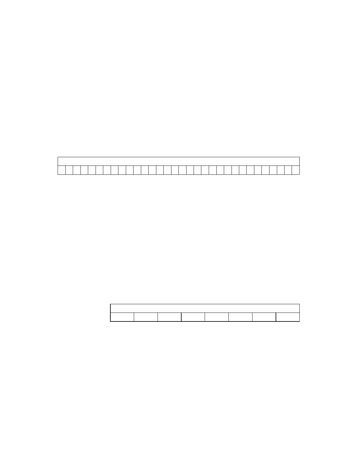
Temporary (TEMP)
Read/Write
TEMP
Temporary
[31:0]
This 32-bit register stores the Return instruction address
pointer from the Call instruction. The address pointer
stored in this register is loaded into the
register when a Return instruction is
executed. This address points to the next instruction to
execute. Do not write to this register while the
LSI53C895A is executing SCRIPTS.
During any Memory-to-Memory Move operation, the
contents of this register are preserved. The power-up
value of this register is indeterminate.
Register: 0x20
DMA FIFO (DFIFO)
Read/Write
BO
Byte Offset Counter
[7:0]
These bits, along with bits [1:0] in the
register, indicate the amount of data
transferred between the SCSI core and the DMA core. It
is used to determine the number of bytes in the DMA
FIFO when an interrupt occurs. These bits are unstable
while data is being transferred between the two cores.
31
0
TEMP
x
x
x
x
x
x
x
x
x
x
x
x
x
x
x
x
x
x
x
x
x
x
x
x
x
x
x
x
x
x
x
x
7
0
BO
0
0
0
0
0
0
0
0