Cpu interface, Cpu interface –41 – Altera CPRI IP Core User Manual
Page 73
Chapter 4: Functional Description
4–41
CPU Interface
December 2013
Altera Corporation
CPRI MegaCore Function
User Guide
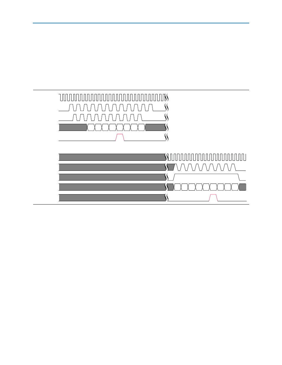
shows an example timing diagram in which an input error is noted on the
MII of a transmitting RE or REC master, and the data from the MII is transmitted on
the CPRI link to a receiving RE slave. The timing diagram shows the MII signals on
the transmitting master and the receiving slave. The data value captured on the MII
transmitter module of the RE or REC master when
cpri_mii_txer
is asserted, is
passed to the CPRI link as a 5-bit Ethernet HALT symbol (5’b00100). The RE slave MII
receiver module decodes this symbol as an F (4’b1111) while the
cpri_mii_rxer
signal
is asserted.
For more information about the MII receiver module, refer to
.
CPU Interface
Use the CPU interface to communicate the contents of the control word of a CPRI
hyperframe — VSS, Ethernet, High-Level Data Link Controller (HDLC), and
synchronization and timing information — and to access status and configuration
information in the CPRI IP core registers. An on-chip processor such as the Nios II
processor, or an external processor, can access the CPRI configuration address space
using this interface.
The CPU interface provides an Avalon-MM slave interface that accesses all registers in
the CPRI IP core. The Avalon-MM slave executes transfers between the CPRI IP core
and the user-defined logic in your design.
f
For information about the Avalon-MM interface, refer to
Figure 4–24. CPRI MII Signals on Transmitting RE or REC Master and on Receiving RE Slave
cpri_mii_txclk
cpri_mii_txrd
cpri_mii_txen
cpri_mii_txd[3:0]
cpri_mii_txer
cpri_mii_rxclk
cpri_mii_rxwr
cpri_mii_rxdv
cpri_mii_rxd[3:0]
D0
D1
D2
D3
D4
D5
D6
D7
D0
K
D1
D2
D3
F
D5
D6
D7
cpri_mii_rxer