Rainbow Electronics W90P710CDG User Manual
Page 84
W90P710CD/W90P710CDG
- 84 -
BITS
DESCRIPTION
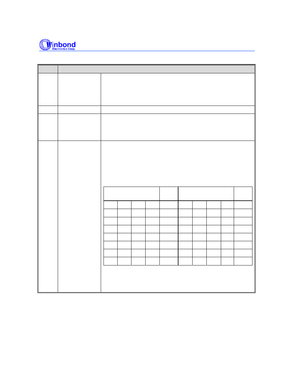
[31:16] DLH_CLK_REF
Latch DLH_CLK clock tree by HCLK positive edge
The SDRAM MCLK is generated by inserting a delay (XOR2) chain in
HCLK positive or negedge edge to adjust the MCLK skew. So software
can read these bits to expore MCLK and HCLK relationship. [31:24] is
used for positive edge and [23:16] is for negedge edge.
[15:9] RESERVED -
[8] SWPON
SDRAM Initialization by Software
Set this bit “1” will issue a SDRAM power on default setting command
sequence like system power on, this bit will be auto-clear by hardware
while SDRAM initialization finish.
[7:4] DLH_CLK_SKEW
Data latch Clock Skew Adjustment
Due to PC board loading or too many devices connect to external
address and data bus, it may causes SDRAM can not work correctly at
high frequency (usually, > 80MHz) software can control
MCLK_O_D[3:0] to adjust address and data bus to adjust setup/hold
time.
DLH_CLK_SKEW[7:4]
Gate
Delay
DLH_CLK_SKEW[7:4] Gate
Delay
0 0 0 0 P-0 1 0 0 0 N-0
0 0 0 1 P-1 1 0 0 1 N-1
0 0 1 0 P-2 1 0 1 0 N-2
0 0 1 1 P-3 1 0 1 1 N-3
0 1 0 0 P-4 1 1 0 0 N-4
0 1 0 1 P-5 1 1 0 1 N-5
0 1 1 0 P-6 1 1 1 0 N-6
0 1 1 1 P-7 1 1 1 1 N-7
NOTE: P-x means Data latched Clock shift “X” gates delays by refer
MCLKO positive edge, N-x means Data latched Clock shift “X” gates
delays by refer MCLKO negative edge.