Rainbow Electronics W90P710CDG User Manual
Page 303
W90P710CD/W90P710CDG
Publication Release Date: September 19, 2006
- 303 -
Revision B2
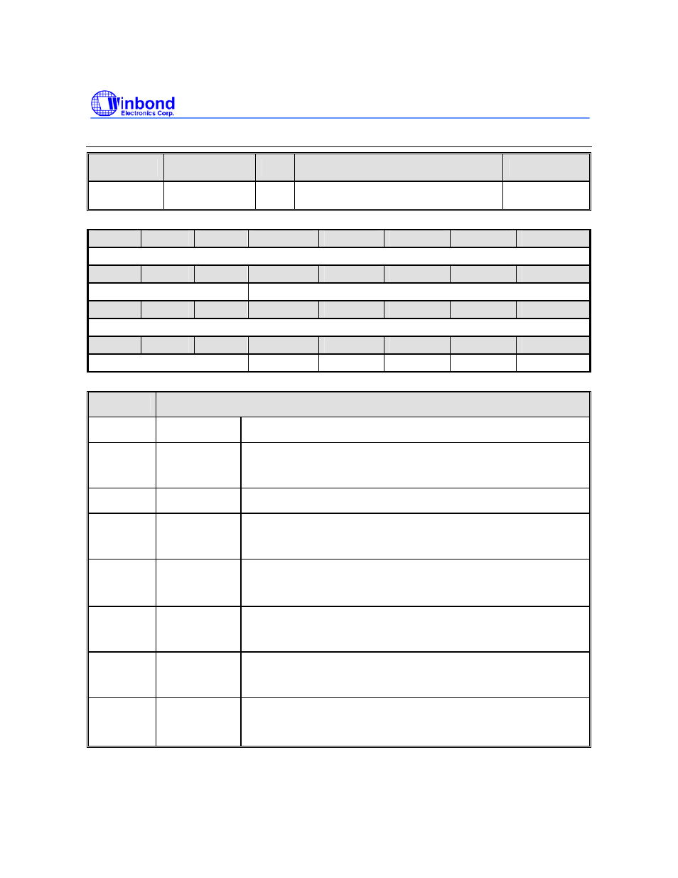
LCD Timing Control 5 Register (LCDTCON5)
REGISTER
ADDRESS
R/W
DESCRIPTION
RESET VALUE
LCDTCON5 0xFFF0_80C0
R/W LCD Timing Control 5
0x0000_0000
31
30
29
28
27
26
25
24
Reserved
23
22
21
20
19
18
17
16
Reserved ACBF
15
14
13
12
11
10
9
8
Reserved
7
6
5
4
3
2
1
0
Reserved MMODE
INVVCLK
INVHSYN
INVVSYN INVVDEN
BITS
DESCRIPTIONS
[31:21] Reserved
Reserved
[20:16] ACBF
Determine the toggle rate of the VDEN AC bias pin).The AC bias pin
frequency is only applicable to STN display. Program this field with
the number of line clocks between each toggle.
[15:5] Reserved Reserved
[4] MMODE
Determine the toggle rate of the VDEN
0 = Each Frame
1 = The rate defined by the ACBF.
[3] INVVCLK
This bit controls the polarity of the VCLK active edge.
0 = Panel signal is transit at VCLK rising edge
1 = Panel signal is transit at VCLK falling edge
[2] INVHSYNC
This bit indicates the HSYNC pulse polarity.
0 = Normal
1 = Inverted
[1] INVVSYNC
This bit indicates the VSYNC pulse polarity.
0 = Normal
1 = Inverted
[0] INVVDEN
This bit indicates the VDEN signal polarity.
0 = Normal
1 = Inverted