Pin description – Rainbow Electronics W90P710CDG User Manual
Page 20
W90P710CD/W90P710CDG
- 20 -
5. PIN
DESCRIPTION
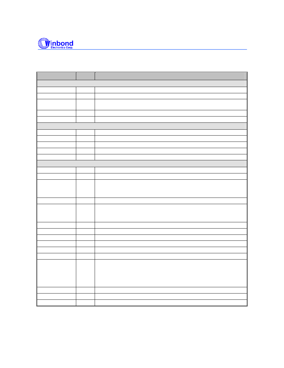
Table 5.1 W90P710 Pins Description
PIN NAME
IO TYPE
DESCRIPTION
Clock & Reset
EXTAL (15M)
I
15MHz External Clock / Crystal Input
XTAL (15M)
O
15MHz Crystal Output
EXTAL32(32.768
K)
I
32768Hz External Clock / Crystal Input(for RTC)
XTAL32(32.768K) O 32768Hz
Crystal Output(for RTC)
nRESET
IS
System Reset, active-low
JTAG Interface
TCK
IDS
JTAG Test Clock, internal pull-down with 58K ohm
TMS
IUS
JTAG Test Mode Select, internal pull-up with 70K ohm
TDI
IUS
JTAG Test Data in, internal pull-up with 70K ohm
TDO
O
JTAG Test Data out
nTRST
IUS
JTAG Reset, active-low, internal pull-up with 70K ohm
External Bus Interface
A [21:18]
O
Address Bus (MSB) of external memory and IO devices.
A [17:0]
IOS
Address Bus of external memory and IO devices.
D [31:16] /
VD[23:8] /
GPIO [67:52]
IOU
Data Bus (MSB) of external memory and IO device, internal pull-up with 70K
ohm.
General Programmable In/Out Port GPIO[67:52].
D [15:0] /
IOU
Data Bus (LSB) of external memory and IO device.
nWBE [3:0] /
SDQM [3:0] /
GPIO[69:68]
IOU
Write Byte Enable for specific device (nECS [3:0]).
Data Bus Mask signal for SDRAM (nSCS [1:0]), active-low.
General Programmable In/Out Port [69:68]
nSCS [1:0]
O
SDRAM chip select for two external banks, active-low.
nSRAS
O
Row Address Strobe for SDRAM, active-low.
nSCAS
O
Column Address Strobe for SDRAM, active-low.
nSWE
O
SDRAM Write Enable, active-low
MCKE
O
SDRAM Clock Enable, active-high
MCLK
O
System Master Clock Out, SDRAM clock, output with slew-rate control
nWAIT /
GPIO[70] /
nIRQ5
IOU
External Wait, active-low.
This pin indicates that the external devices need more active cycle during
access operation.
General Programmable In/Out Port GPIO[70]. If memory and IO devices in EBI
do not need wait request, it can be configured as GPIO[7] or nIRQ5
nBTCS
O
ROM/Flash Chip Select, active-low.
nECS [3:0]
O
External I/O Chip Select, active-low.
nOE
O
ROM/Flash, External Memory Output Enable, active-low.