Rainbow Electronics W90P710CDG User Manual
Page 52

W90P710CD/W90P710CDG
- 52 -
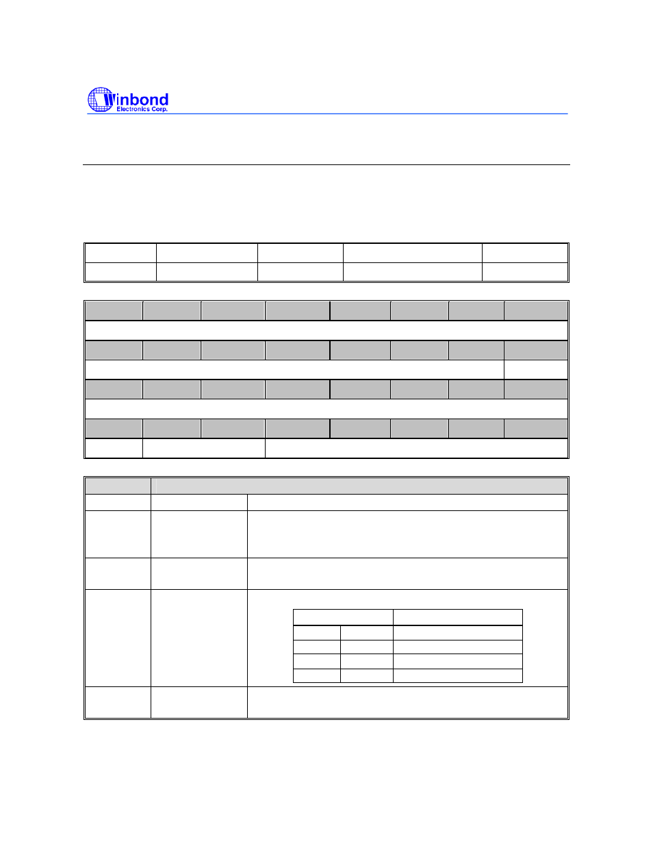
PLL Control Register0 (PLLCON0)
W90P710 provides two clock generation options – crystal and oscillator. The external clock via
EXTAL(15M) Minput pin as the reference clock input of PLL module. The external clock can bypass the
PLL and be used to the internal system clock by pull-down the data D15 pin. Using PLL’s output clock
for the internal system clock, D15 pin must be pull-up.
REGISTER ADDRESS
R/W
DESCRIPTION RESET
VALUE
PLLCON
0xFFF0_0008 R/W
PLL Control Register
0x0000_2F01
31
30
29
28
27
26
25
24
RESERVED
23
22
21
20
19
18
17
16
RESERVED PWDEN
15
14
13
12
11
10
9
8
FBDV
7
6
5
4
3
2
1
0
FBDV OTDV
INDV
BITS
DESCRIPTION
[31:17] RESERVED
-
[16] PWDEN
Power down mode enable
0 = PLL is in normal mode (default)
1 = PLL is in power down mode
[15:7] FBDV
PLL VCO output clock feedback divider
Feedback Divider divides the output clock from VCO of PLL.
[6:5] OTDV
PLL output clock divider
OTDV [6:5]
DIVIDED BY
0 0
1
0 1
2
1 0
2
1 1
4
[4:0] INDV
PLL input clock divider
Input divider divides the input reference clock into the PLL.
