Rainbow Electronics W90P710CDG User Manual
Page 479
W90P710CD/W90P710CDG
Publication Release Date: September 19, 2006
- 479 -
Revision B2
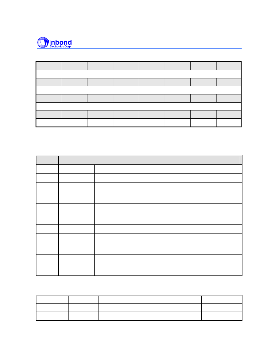
31
30
29
28
27
26
25
24
Reserved
23
22
21
20
19
18
17
16
Reserved
15
14
13
12
11
10
9
8
Reserved
7
6
5
4
3
2
1
0
Reserved
Reserved
SDR
SCR
Reserved
SDW
SCW
Note: This register is used as software mode of I
2
C. Software can read/write this register no matter
I2C_EN is 0 or 1. But SCL and SDA are controlled by software only when I2C_EN = 0.
BITS
DESCRIPTIONS
[31:6]
Reserved
Reserved
[5]
Reserved
Reserved
[4]
SDR
Serial Interface SDA Status (Read only)
0 = SDA is Low.
1 = SDA is High.
[3]
SCR
Serial Interface SCK Status (Read only)
0 = SCL is Low.
1 = SCL is High.
[2]
Reserved
Reserved
[1]
SDW
Serial Interface SDA Output Control
0 = SDA pin is driven Low.
1 = SDA pin is tri-state.
[0]
SCW
Serial Interface SCK Output Control
0 = SCL pin is driven Low.
1 = SCL pin is tri-state.
I2C Data Receive Register 0/1 (I2C_RxR 0/1)
REGISTER OFFSET
R/W
DESCRIPTION
RESET
VALUE
I2C_RXR0
0xFFF8_6010
R
I2C Data Receive Register 0
0x0000_0000
I2C_RXR1
0xFFF8_6110
R
I2C Data Receive Register 1
0x0000_0000