FUJITSU MB91F109 FR30 User Manual
Page 99
75
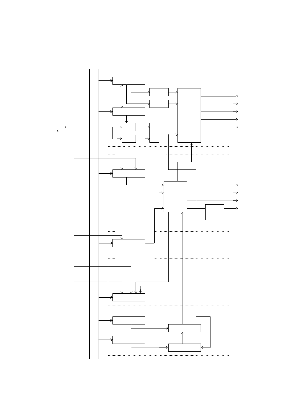
3.1 Outline of Clock Generator and Controller
■
Clock Generator and Controller Block Diagram
Figure 3.1.2 is a block diagram of the clock generator and controller.
Figure 3.1-2 Block Diagram of the Clock Generator and Controller
X0
PLL
X1
1/2
R
|
B
U
S
[Gear controller]
GCR register
CPU gear
Peripheral
gear
PCTR register
Oscilla-
tion
circuit
Selector circuit
Internal
clock
generation
circuit
CPU clock
Internal bus clock
External bus clock
Peripheral
DMA clock
Internal peripheral
clock
[Stop/sleep controller]
Internal interrupt
Internal reset
STCR register
CPU hold permission
Status
transition
control
circuit
Stop state
Sleep state
CPU hold request
Internal reset
Reset
generation
F/F
[DMA suppression
circuit]
DMA request
PDRR register
[Reset reason circuit]
Power-on reset
RSTX pin
RSRR register
[Watchdog controller]
WPR register
Watchdog F/F
CTBR register
Timebase timer
Count clock
- XG Series P3NK-4452-01ENZD (614 pages)
- FPCAC14C (1 page)
- MCJ3230SS (161 pages)
- MBA3073NC (138 pages)
- T5140 (102 pages)
- T5140 (76 pages)
- MAM3367MC/MP (152 pages)
- MPC3045AH (185 pages)
- MB2142-02 (23 pages)
- MB15F86UL (6 pages)
- MHS2030AT (40 pages)
- MHW2100BS (296 pages)
- MHK2060AT (227 pages)
- Disk Drives MHK2060AT (227 pages)
- MCM3064SS (170 pages)
- Mainboard D1561 (45 pages)
- MHC2040AT (219 pages)
- D1961 (45 pages)
- DISK DRIVES MHM2100AT (231 pages)
- MHR2010AT (250 pages)
- MHZ2120BJ (320 pages)
- MCE3064AP (175 pages)
- LQFP-64P (16 pages)
- Solaris PCI GigabitEthernet 3.0 (115 pages)
- MAY2036RC (94 pages)
- MAB3091 (142 pages)
- MPE3XXXAT (191 pages)
- MHV2040AH (40 pages)
- MHW2040AC (278 pages)
- ETERNUSmgr P2X0-0202-01EN (64 pages)
- VSS Hardware Provider 2.1 (134 pages)
- MAG3182FC (61 pages)
- MAU3147NC/NP (130 pages)
- MAX3147RC (94 pages)
- MHV2160BT (296 pages)
- MHV2040AT (280 pages)
- MAW3300NC/NP (130 pages)
- DeskPower E623 (50 pages)
- MAG3182LC (133 pages)
- OPTICAL DISK DRIVES MDG3064UB (42 pages)
- MHF2021AT (225 pages)
- MHR2040AT (40 pages)
- Single Drive FTM7926FB (1 page)
- PG-FCS103 (98 pages)
- MAS3735FC (114 pages)