5 read and write combination cycles – FUJITSU MB91F109 FR30 User Manual
Page 194
170
CHAPTER 4 BUS INTERFACE
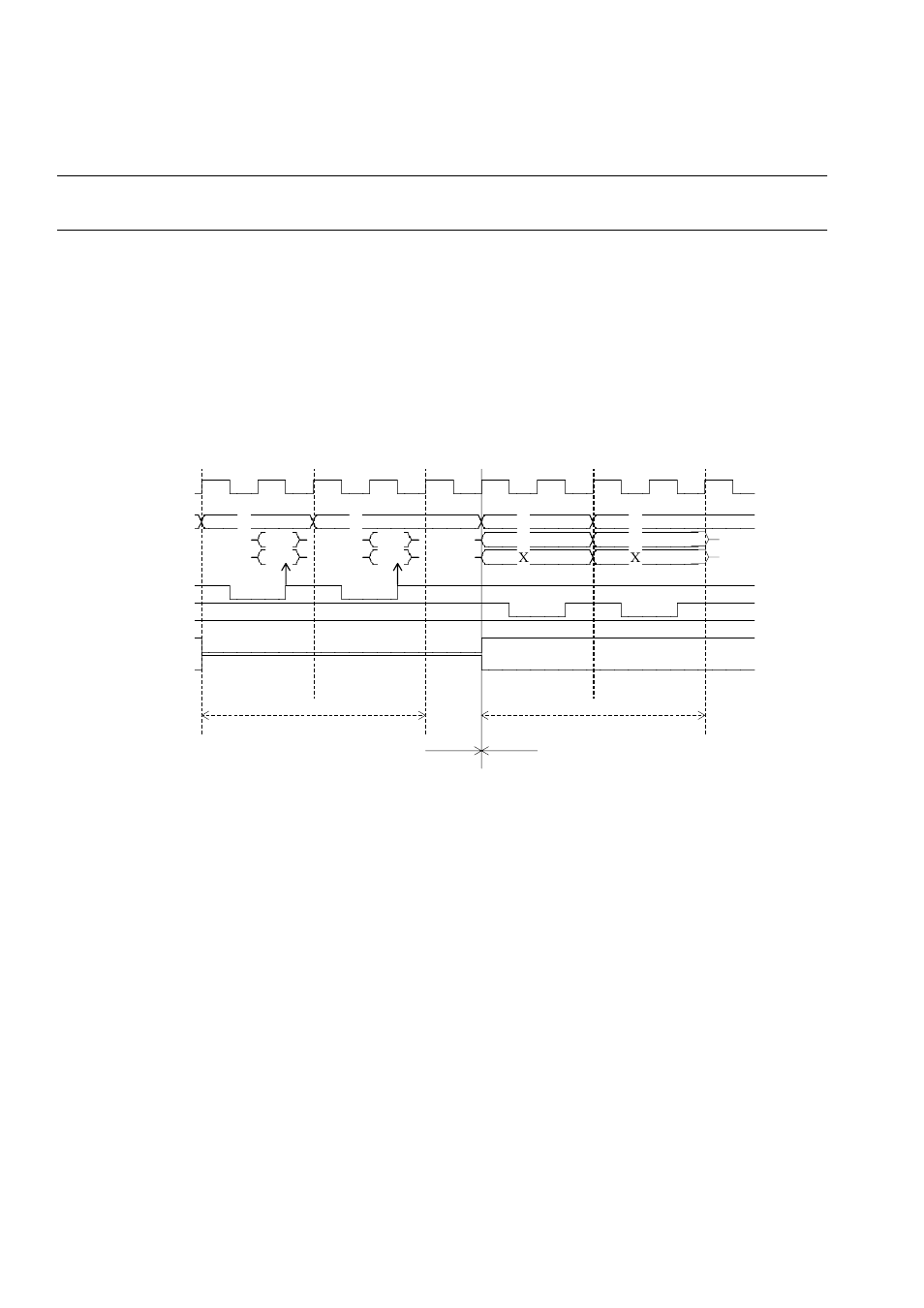
4.17.5 Read and Write Combination Cycles
This section provides a read and write combination cycle timing chart.
■
Read and Write Combination Cycle Timing Chart
❍
CS0 area: 16-bit bus width, word read
CS1 area: 8-bit bus width, half-word read
Figure 4.17-13 Example of Read and Write Combination Cycle Timing Chart
[Explanation of operation]
•
The above example shows the case, where an idle cycle (idle bus cycle) is inserted in
between the chip select areas. When an idle cycle is inserted in between bus cycles, the
address of the previous bus cycle is output as is until the next bus cycle starts. Because of
this, CS0 to CS5X, which corresponds to the output address, are continuously asserted.
•
The above example is a combination of 16-bit and 8-bit data buses.
As the maximum bus width is 16 bits, D23 to D16 and WR1X do not become I/O ports even
in the 8-bit access area (the CS1 area). D23 to D16 output indefinite data, and WR1X is
negated.
BA1
CLK
A24-00
#0
#2
#0
#1
D31-24
#0
#2
#0
#1
D23-16
#1
#3
RDX
WR0X
WR1X
CS0X
CS1X
Word read cycle
Half-word write cycle
CS0 area
CS1 area
BA2
BA1
BA1
BA1
BA2
BA2
BA
Idle
Idle