4 dram relationships – FUJITSU MB91F109 FR30 User Manual
Page 179
155
4.16 Relationship between Data Bus Widths and Control Signals
4.16.4 DRAM Relationships
This section explains the DRAM relationships.
■
DRAM Control Pins
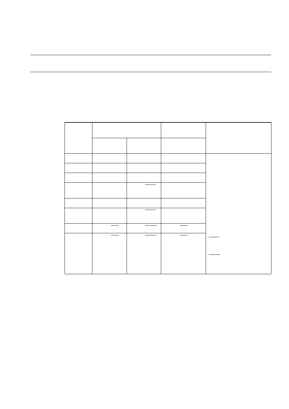
Table 4.16-2 lists the relationship between the pin functions and bus widths used in the DRAM
interface.
Table 4.16-2 Functions and Bus Widths of DRAM Control Pins
Pin name
Data bus in 16-bit mode
Data bus in 8-bit
mode
Remarks
2CAS/1WE
mode
1CAS/2WE
mode
RAS0
Area 4 RAS
Area 4 RAS
Area 4 RAS
•
Correspondence
between "L" and "H"
and lower 1 bit (A0) of
address for data bus in
16-bit mode
•
"L":"0"
•
"H":"1"
CASL: CAS corresponding
to area containing
"0" in A0
CASH: CAS
corresponding
to area containing
"1" in A0
WEL: WE corresponding
to area containing
"0" in A0
WEH: WE corresponding
to area containing
"1" in A0
RAS1
Area 5 RAS
Area 5 RAS
Area 5 RAS
CS0L
Area 4 CASL
Area 4 CAS
Area 4 CAS
CS0H
Area 4
CASH
Area 4 WEL
Area 4 CAS
CS1L
Area 5 CASL
Area 5 CAS
Area 5 CAS
CS1H
Area 5
CASH
Area 5 WEL
Area 5 CAS
DW0X
Area 4 WE
Area 4 WEH
Area 4 WE
DW1X
Area 5 WE
Area 5 WEH
Area 5 WE
- XG Series P3NK-4452-01ENZD (614 pages)
- FPCAC14C (1 page)
- MCJ3230SS (161 pages)
- MBA3073NC (138 pages)
- T5140 (102 pages)
- T5140 (76 pages)
- MAM3367MC/MP (152 pages)
- MPC3045AH (185 pages)
- MB2142-02 (23 pages)
- MB15F86UL (6 pages)
- MHS2030AT (40 pages)
- MHW2100BS (296 pages)
- MHK2060AT (227 pages)
- Disk Drives MHK2060AT (227 pages)
- MCM3064SS (170 pages)
- Mainboard D1561 (45 pages)
- MHC2040AT (219 pages)
- D1961 (45 pages)
- DISK DRIVES MHM2100AT (231 pages)
- MHR2010AT (250 pages)
- MHZ2120BJ (320 pages)
- MCE3064AP (175 pages)
- LQFP-64P (16 pages)
- Solaris PCI GigabitEthernet 3.0 (115 pages)
- MAY2036RC (94 pages)
- MAB3091 (142 pages)
- MPE3XXXAT (191 pages)
- MHV2040AH (40 pages)
- MHW2040AC (278 pages)
- ETERNUSmgr P2X0-0202-01EN (64 pages)
- VSS Hardware Provider 2.1 (134 pages)
- MAG3182FC (61 pages)
- MAU3147NC/NP (130 pages)
- MAX3147RC (94 pages)
- MHV2160BT (296 pages)
- MHV2040AT (280 pages)
- MAW3300NC/NP (130 pages)
- DeskPower E623 (50 pages)
- MAG3182LC (133 pages)
- OPTICAL DISK DRIVES MDG3064UB (42 pages)
- MHF2021AT (225 pages)
- MHR2040AT (40 pages)
- Single Drive FTM7926FB (1 page)
- PG-FCS103 (98 pages)
- MAS3735FC (114 pages)