12 automatic wait cycles in usual dram interface – FUJITSU MB91F109 FR30 User Manual
Page 205
181
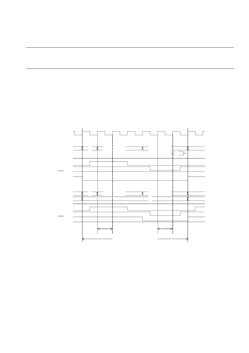
4.17 Bus Timing
4.17.12 Automatic Wait Cycles in Usual DRAM Interface
This section provides an automatic wait cycle timing chart in the usual DRAM
interface.
■
Automatic Wait Cycle Timing Chart in Usual DRAM Interface
❍
Bus width: 8 bits, access: bytes
Figure 4.17-24 Example of Automatic Wait Cycle Timing Chart in Usual DRAM Interface
[Explanation of operation]
•
When adding only one wait clock cycle to the Q1 and Q4 cycles, set the Q1W and Q4W bits
of DMCR4 and DMCR5. The inserted cycles are called the "Q1W" and "Q4W" cycles.
The Q1W and Q4W cycles execute the same cycles as the Q1 and Q4 cycles. By this
operation, the "H" width of RAS and the "L" width of CAS can be extended by one cycle,
respectively.
Set the widths according to the DRAM access time.
Q1
Q1W
Q2
Q3
Q4
Q4W
Q5
CLK
1)Read
A24-00
X
#0 row.adr.
#0 col.adr.
D31-24
#0
D23-16
RAS
CAS
WE
RDX
2)Write
A24-00
X
#0 row.adr.
#0 col.adr.
D31-24
#0
D23-16
RAS
CAS
WE
RDX
Q1 wait
Q4 wait
Usual DRAM interface
- XG Series P3NK-4452-01ENZD (614 pages)
- FPCAC14C (1 page)
- MCJ3230SS (161 pages)
- MBA3073NC (138 pages)
- T5140 (102 pages)
- T5140 (76 pages)
- MAM3367MC/MP (152 pages)
- MPC3045AH (185 pages)
- MB2142-02 (23 pages)
- MB15F86UL (6 pages)
- MHS2030AT (40 pages)
- MHW2100BS (296 pages)
- MHK2060AT (227 pages)
- Disk Drives MHK2060AT (227 pages)
- MCM3064SS (170 pages)
- Mainboard D1561 (45 pages)
- MHC2040AT (219 pages)
- D1961 (45 pages)
- DISK DRIVES MHM2100AT (231 pages)
- MHR2010AT (250 pages)
- MHZ2120BJ (320 pages)
- MCE3064AP (175 pages)
- LQFP-64P (16 pages)
- Solaris PCI GigabitEthernet 3.0 (115 pages)
- MAY2036RC (94 pages)
- MAB3091 (142 pages)
- MPE3XXXAT (191 pages)
- MHV2040AH (40 pages)
- MHW2040AC (278 pages)
- ETERNUSmgr P2X0-0202-01EN (64 pages)
- VSS Hardware Provider 2.1 (134 pages)
- MAG3182FC (61 pages)
- MAU3147NC/NP (130 pages)
- MAX3147RC (94 pages)
- MHV2160BT (296 pages)
- MHV2040AT (280 pages)
- MAW3300NC/NP (130 pages)
- DeskPower E623 (50 pages)
- MAG3182LC (133 pages)
- OPTICAL DISK DRIVES MDG3064UB (42 pages)
- MHF2021AT (225 pages)
- MHR2040AT (40 pages)
- Single Drive FTM7926FB (1 page)
- PG-FCS103 (98 pages)
- MAS3735FC (114 pages)