2 pwm timer block diagram – FUJITSU MB91F109 FR30 User Manual
Page 326
302
CHAPTER 14 PWM TIMER
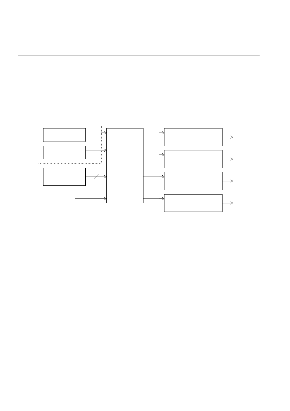
14.2 PWM Timer Block Diagram
Figure 14.2-1 is a general block diagram of the PWM timer. Figure 14.2-2 is a block
diagram of a single PWM timer channel.
■
General Block Diagram of PWM Timer
Figure 14.2-1 General Block Diagram of PWM Timer
PWM0
PWM1
4
PWM2
PWM3
16-bit reload
timer ch0
16-bit reload
timer ch1
General control
register 2
External TRGs 0 to 3
General control register 1
(source selection)
TRG input PWM timer
ch0
TRG input PWM timer
ch1
TRG input PWM timer
ch2
TRG input PWM timer
ch3
See also other documents in the category FUJITSU Hardware:
- XG Series P3NK-4452-01ENZD (614 pages)
- FPCAC14C (1 page)
- MCJ3230SS (161 pages)
- MBA3073NC (138 pages)
- T5140 (102 pages)
- T5140 (76 pages)
- MAM3367MC/MP (152 pages)
- MPC3045AH (185 pages)
- MB2142-02 (23 pages)
- MB15F86UL (6 pages)
- MHS2030AT (40 pages)
- MHW2100BS (296 pages)
- MHK2060AT (227 pages)
- Disk Drives MHK2060AT (227 pages)
- MCM3064SS (170 pages)
- Mainboard D1561 (45 pages)
- MHC2040AT (219 pages)
- D1961 (45 pages)
- DISK DRIVES MHM2100AT (231 pages)
- MHR2010AT (250 pages)
- MHZ2120BJ (320 pages)
- MCE3064AP (175 pages)
- LQFP-64P (16 pages)
- Solaris PCI GigabitEthernet 3.0 (115 pages)
- MAY2036RC (94 pages)
- MAB3091 (142 pages)
- MPE3XXXAT (191 pages)
- MHV2040AH (40 pages)
- MHW2040AC (278 pages)
- ETERNUSmgr P2X0-0202-01EN (64 pages)
- VSS Hardware Provider 2.1 (134 pages)
- MAG3182FC (61 pages)
- MAU3147NC/NP (130 pages)
- MAX3147RC (94 pages)
- MHV2160BT (296 pages)
- MHV2040AT (280 pages)
- MAW3300NC/NP (130 pages)
- DeskPower E623 (50 pages)
- MAG3182LC (133 pages)
- OPTICAL DISK DRIVES MDG3064UB (42 pages)
- MHF2021AT (225 pages)
- MHR2040AT (40 pages)
- Single Drive FTM7926FB (1 page)
- PG-FCS103 (98 pages)
- MAS3735FC (114 pages)