13 dram interface in high-speed page mode – FUJITSU MB91F109 FR30 User Manual
Page 206
182
CHAPTER 4 BUS INTERFACE
4.17.13 DRAM Interface in High-Speed Page Mode
This section provides DRAM interface operation timing charts in high-speed page
mode.
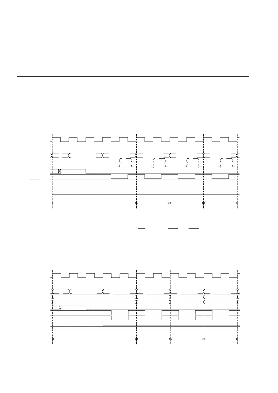
■
DRAM Interface Timing Charts in High-Speed Page Mode
❍
Read cycle, bus width: 16 bits, access: words
Figure 4.17-25 Example 1 of DRAM Interface Timing Chart in High-Speed Page Mode
[Explanation of operation]
•
Read control is performed with only the CAS control signals (including CASL and CASH)
while RAS is lowered to "L", and "H" of WE (including WEL and WEH) is held.
•
Column addresses are output in Q4 and Q5 cycles.
❍
Write cycle, bus width: 16 bits, access: words
Figure 4.17-26 Example 2 of DRAM Interface Timing Chart in High-Speed Page Mode
Q1
Q2
Q3
Q4
Q5
Q4
Q5
Q4
Q5
Q4
Q5
CLK
1CAS/2WE
A24-00
X
#0 row.adr.
#0 col.adr
#2 col.adr
#4 col.adr
#6 col.adr
D31-24
#0
#2
#4
#6
D23-16
#1
#3
#5
#7
RAS
CAS
WEL
WEH
RDX
1)
Usual DRAM bus cycle
High-speed page High-speed page High-speed page
Q1
Q2
Q3
Q4
Q5
Q4
Q5
Q4
Q5
Q4
Q5
CLK
2CAS/1WE
A24-00
X
#0 row.adr.
#0 col.adr
#2 col.adr
#4 col.adr
#6 col.adr
D31-24
#0
#2
#4
#6
D23-16
#1
#3
#5
#7
RAS
CASL
CASH
WE
RDX
2)
Usual DRAM bus cycle
High-speed page High-speed page High-speed page