11 refresh control register (rfcr) – FUJITSU MB91F109 FR30 User Manual
Page 154
130
CHAPTER 4 BUS INTERFACE
4.11 Refresh Control Register (RFCR)
The refresh control register (RFCR) controls the CBR (CAS before RAS) refresh
operation when the DRAM interface is used.
This register has a 6-bit downward counter that uses the divide-by-32 output of a
timebase timer as a clock source and specifies a refresh interval by controlling its
reload value by the RFCR.
■
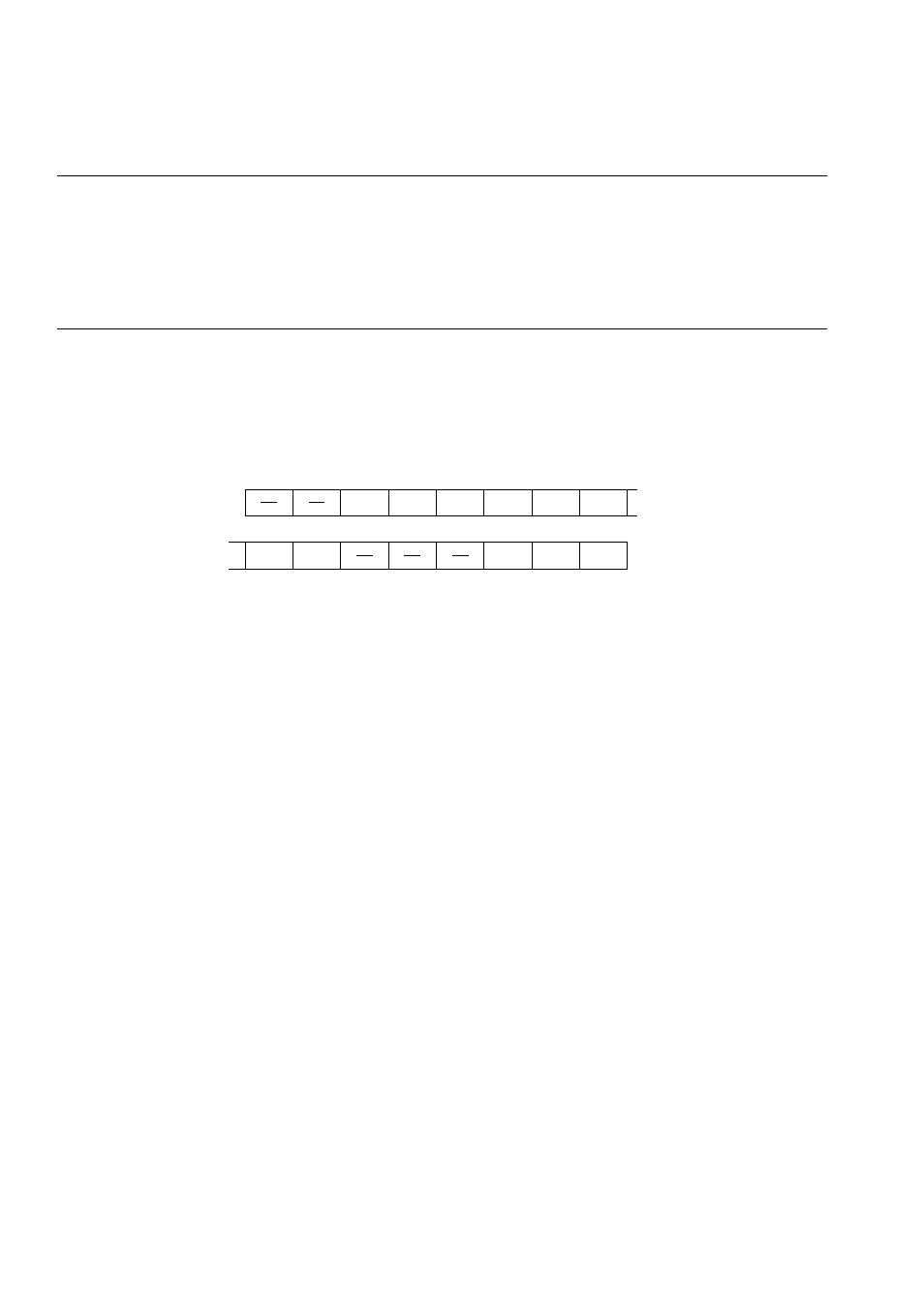
Configuration of Refresh Control Register (RFCR)
The refresh control register (RFCR) is configured as follows:
The timebase timer is a counter used for oscillation stabilization wait intervals. It operates with
a frequency that is one half of X0 when CHC=1 is set by the gear control register (GCR) and
with a frequency equal to the internal PLL oscillation frequency when CHC=0. For example,
when the PLL oscillation frequency is 25 MHz at CHC=0, one cycle equals 40 ns, and 40 × 32 =
1280 ns equals one refresh interval.
The refresh interval is counted with the output from the timebase timer.
■
Bit Functions of Refresh Control Register (RFCF)
[bit 13 to 8] REL (RELoad value bits)
The REL is a register to set refresh intervals.
At read time, the count of the refresh interval downward counter is read as is.
The DRAMs of areas 4 and 5 are refreshed at the same time with the interval indicated by
the REL.
[bit 7] R1W (Refresh 1 Wait)
The R1W bit extends the first refresh cycle (R1) by only one cycle.
0: no wait (initial value)
1: wait
[bit 6] R3W (Refresh 3 Wait)
The R3W bit extends the third refresh cycle (R3) by one cycle.
0: no wait (initial value)
1: wait
15
14
13
12
11
10
9
8
RFCR
REL5 REL4 REL3 REL2 REL1 REL0
--XXXXXX
R/W
Address: 0000 0626
H
7
6
5
4
3
2
1
0
R1W
R3W
STR
CKS1 CKS0
00---000
R/W
Initial value
Initial value
Access
Access