15 single dram interface: write – FUJITSU MB91F109 FR30 User Manual
Page 210
186
CHAPTER 4 BUS INTERFACE
4.17.15 Single DRAM Interface: Write
This section provides a single DRAM interface write timing chart.
■
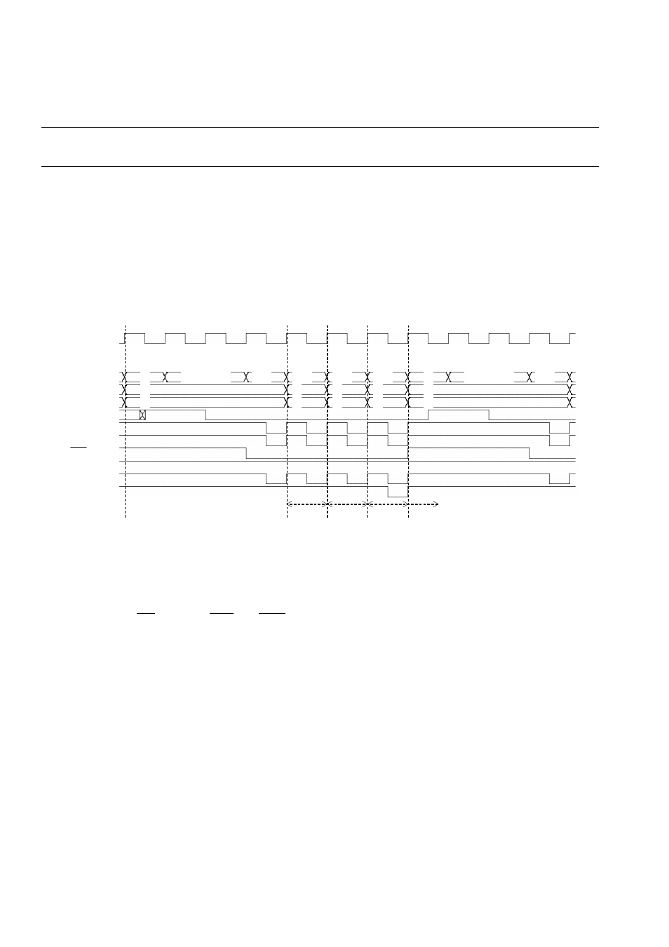
Single DRAM Interface: Write Timing Chart
❍
Bus width: 16 bits, access: words
Figure 4.17-30 Example of Single DRAM Interface Write Timing Chart
[Explanation of operation]
•
Column addresses and write data are output in Q4SW cycles.
•
CAS is asserted at the falling edge of Q4SW and negated at the rising edge or end of the
Q4SW cycle.
•
WE (including WEL and WEH) is asserted at the rising edge of the Q4SW cycle and negated
when Q4SW ends.
Q1
Q2
Q3
Q4SW
Q4SW
Q4SW
Q4SW
Q1
Q2
Q3
Q4SW
CLK
2)2CAS/1WE
A24-00
X
row.adr.
col.
col.
col.
col.
X
row.adr.
col.
D31-24
W
W
W
W
W
D23-16
W
W
W
W
W
RAS
CASL
CASH
WE
RDX
(DACK0)
(EOP0)
High speed
page
High speed
page
High speed
page
See also other documents in the category FUJITSU Hardware:
- XG Series P3NK-4452-01ENZD (614 pages)
- FPCAC14C (1 page)
- MCJ3230SS (161 pages)
- MBA3073NC (138 pages)
- T5140 (102 pages)
- T5140 (76 pages)
- MAM3367MC/MP (152 pages)
- MPC3045AH (185 pages)
- MB2142-02 (23 pages)
- MB15F86UL (6 pages)
- MHS2030AT (40 pages)
- MHW2100BS (296 pages)
- MHK2060AT (227 pages)
- Disk Drives MHK2060AT (227 pages)
- MCM3064SS (170 pages)
- Mainboard D1561 (45 pages)
- MHC2040AT (219 pages)
- D1961 (45 pages)
- DISK DRIVES MHM2100AT (231 pages)
- MHR2010AT (250 pages)
- MHZ2120BJ (320 pages)
- MCE3064AP (175 pages)
- LQFP-64P (16 pages)
- Solaris PCI GigabitEthernet 3.0 (115 pages)
- MAY2036RC (94 pages)
- MAB3091 (142 pages)
- MPE3XXXAT (191 pages)
- MHV2040AH (40 pages)
- MHW2040AC (278 pages)
- ETERNUSmgr P2X0-0202-01EN (64 pages)
- VSS Hardware Provider 2.1 (134 pages)
- MAG3182FC (61 pages)
- MAU3147NC/NP (130 pages)
- MAX3147RC (94 pages)
- MHV2160BT (296 pages)
- MHV2040AT (280 pages)
- MAW3300NC/NP (130 pages)
- DeskPower E623 (50 pages)
- MAG3182LC (133 pages)
- OPTICAL DISK DRIVES MDG3064UB (42 pages)
- MHF2021AT (225 pages)
- MHR2040AT (40 pages)
- Single Drive FTM7926FB (1 page)
- PG-FCS103 (98 pages)
- MAS3735FC (114 pages)