FUJITSU MB91F109 FR30 User Manual
Page 30
6
CHAPTER 1 OVERVIEW
1.2
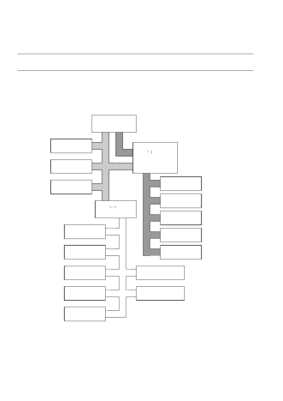
General Block Diagram of MB91F109
Figure 1.2.1 is a general MB91F109 block diagram.
■
General Block Diagram of MB91F109
Figure 1.2-1 General Block Diagram of MB91F109
Notes:
•
Terminals are represented by the function (some terminals are actually multiplexed).
•
When REALOS is used, perform time management using an external interrupt or internal
timer.
I-bus(16bit)
C-bus
(32bit)
RAS0 RAS1
CS0L CS1L
EOP0 EOP1 EOP2
16bit
FLASH ROM
254KB
RSTX
INT0-INT3
NMIX
AN0-AN3
AVCC AVRH
D31-D16
A24-A00
RDX
WR0X-1X
D-bus(32bit)
RDY
CLK
BRQ BGRNTX
CS0X-5X
DREQ0 DREQ1 DREQ2
DACK0 DACK1 DACK2
32bit
CS0H CS1H
DW0X DW1X
X0 X1
R-bus
(16bit)
SC0 SC1 SC2
SO0 SO1 SO2
with Baud Rate Timer
AVSS AVRL
SI0 SI1 SI2
UART (3ch)
10bit A/D Converter
(4ch)
PWM Timer (4ch)
Reload Timer
(3 ch)
Port
ATGX
OCPA0-OCPA3
TRG0-3
RAM 2KB
Port 0-B
DRAM Controller
Bus Controller
Bus Converter
Bus Converter
Interrupt Control Unit
Clock Control Unit
(Watch Dog Timer)
DMAC (8ch)
Bit Search Module
RAM 2KB
FR CPU
Harvard
Princeton
- XG Series P3NK-4452-01ENZD (614 pages)
- FPCAC14C (1 page)
- MCJ3230SS (161 pages)
- MBA3073NC (138 pages)
- T5140 (102 pages)
- T5140 (76 pages)
- MAM3367MC/MP (152 pages)
- MPC3045AH (185 pages)
- MB2142-02 (23 pages)
- MB15F86UL (6 pages)
- MHS2030AT (40 pages)
- MHW2100BS (296 pages)
- MHK2060AT (227 pages)
- Disk Drives MHK2060AT (227 pages)
- MCM3064SS (170 pages)
- Mainboard D1561 (45 pages)
- MHC2040AT (219 pages)
- D1961 (45 pages)
- DISK DRIVES MHM2100AT (231 pages)
- MHR2010AT (250 pages)
- MHZ2120BJ (320 pages)
- MCE3064AP (175 pages)
- LQFP-64P (16 pages)
- Solaris PCI GigabitEthernet 3.0 (115 pages)
- MAY2036RC (94 pages)
- MAB3091 (142 pages)
- MPE3XXXAT (191 pages)
- MHV2040AH (40 pages)
- MHW2040AC (278 pages)
- ETERNUSmgr P2X0-0202-01EN (64 pages)
- VSS Hardware Provider 2.1 (134 pages)
- MAG3182FC (61 pages)
- MAU3147NC/NP (130 pages)
- MAX3147RC (94 pages)
- MHV2160BT (296 pages)
- MHV2040AT (280 pages)
- MAW3300NC/NP (130 pages)
- DeskPower E623 (50 pages)
- MAG3182LC (133 pages)
- OPTICAL DISK DRIVES MDG3064UB (42 pages)
- MHF2021AT (225 pages)
- MHR2040AT (40 pages)
- Single Drive FTM7926FB (1 page)
- PG-FCS103 (98 pages)
- MAS3735FC (114 pages)