FUJITSU MB91F109 FR30 User Manual
Page 40
16
CHAPTER 1 OVERVIEW
47
WR1X/P85
F
Note:
WR1X is Hi-Z while it is in reset state. When it is
used as a 16-bit bus, attach a pull-up resistor to
the outside.
[P84 or P85] When WR0X or WR1X is not used,
the pin can be used as a general-purpose I/O port.
48
49
50
CS0X/PA0
CS1X/PA1
CS2X/PA2
F
Chip Select 0 output (Low active)
Chip Select 1 output (Low active)
Chip Select 2 output (Low active)
[PA0, 1, or 2] When the pin is not used for the
above purpose, it can be used as a general-
purpose I/O port.
51
CS3X/PA3/EOP1
F
Chip Select 3 output (Low active)
[EOP1] DMAC EOP1 output (ch1). This function is
valid when DMAC EOP output is enabled.
[PA3] When CS3X and EOP1 are not used, the pin
can be used as a general-purpose I/O port.
52
53
CS4X/PA4
CS5X/PA5
F
Chip Select 4 output (Low active)
Chip Select 5 output (Low active)
[PA4 or 5] When the pin is not used for the above
purpose, it can be used as a general-purpose I/O
port.
54
CLK/PA6
F
System clock output. The pin outputs the same
clock frequency as the external bus operating
frequency.
[PA6] When the pin is not used for this purpose, it
can be used as a general-purpose I/O port.
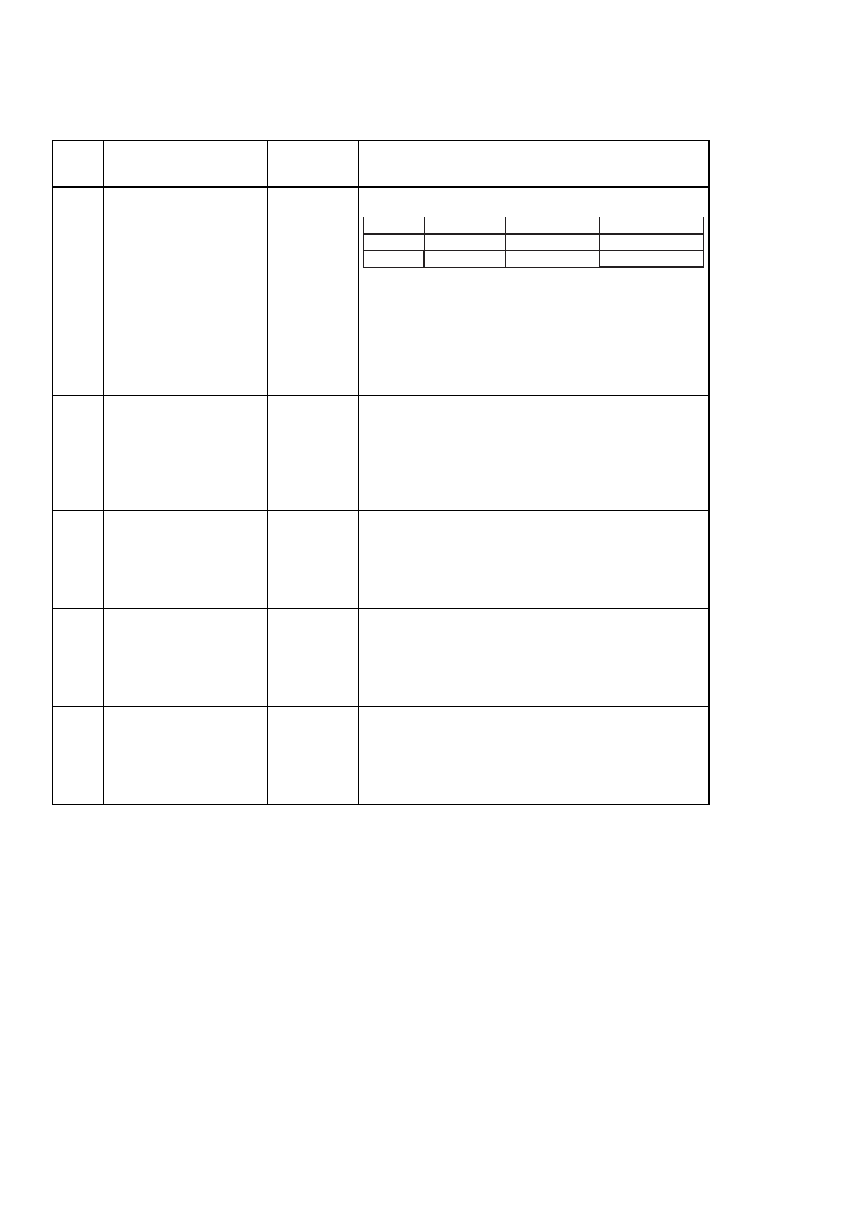
Table 1.5-2 Pin Functions (2/5)
NO.
Pin name
I/O circuit
format
Function
16-bit bus width
8-bit bus width
D15 to D08
D07 to D00
WR0X
WR1X
WR0X
Single-chip mode
(can be used as a port)
(can be used as a port)
(can be used as a port)