15 little endian register (ler) – FUJITSU MB91F109 FR30 User Manual
Page 162
138
CHAPTER 4 BUS INTERFACE
4.15 Little Endian Register (LER)
When bus access by the MB91F109 is performed, the whole area is usually composed
of big endians. However, setting the little endian register (LER) makes it possible to
handle one of areas 1 to 5 as a little endian area.
This register is supported for all bus modes independently of the usual, time sharing,
and DRAM interfaces. However, area 0 is outside the little endian areas.
■
Configuration of Little Endian Register (LER)
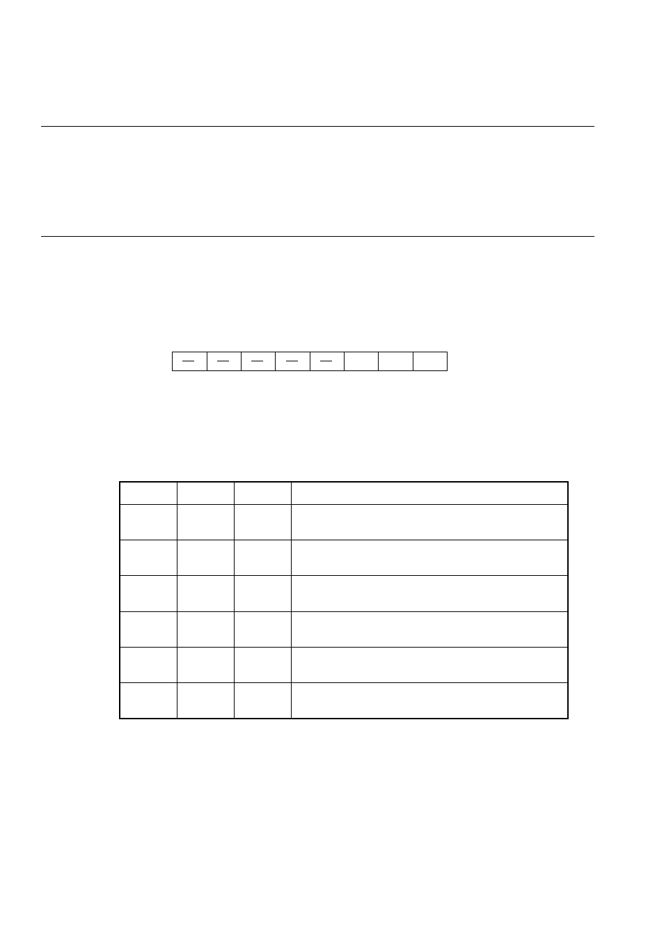
The little endian register (LER) is configured as follows:
■
Bit Functions of Little Endian Register (LER)
As shown in Table 4.15-1, the LE2, LE1, and LE0 bits are combined to specify little endian
areas.
Writing to the LER register can be performed only one time after it is reset.
7
6
5
4
3
2
1
0
LER
Address: 0000 07FE
H
LE2
LE1
LE0
-----000
W
Access
Initial value
Table 4.15-1 Mode Setting Using the Combination of Bits (LE2, LE1, and LE0)
LE2
LE1
LE0
Mode
0
0
0
Initial value after reset.
No little endian area exists.
0
0
1
Area 1 is handled as a little endian.
Areas 0 and 2 to 5 are handled as big endians.
0
1
0
Area 2 is handled as a little endian.
Areas 0 to 1 and 3 to 5 are handled as big endians.
0
1
1
Area 3 is handled as a little endian.
Areas 0 to 2 and 4 to 5 are handled as big endians.
1
0
0
Area 4 is handled as a little endian.
Areas 0 to 3 and 5 are handled as big endians.
1
0
1
Area 5 is handled as a little endian.
Areas 0 to 4 are handled as big endians.