FUJITSU MB91F109 FR30 User Manual
Page 409
385
APPENDIX C Pin Status for Each CPU Status
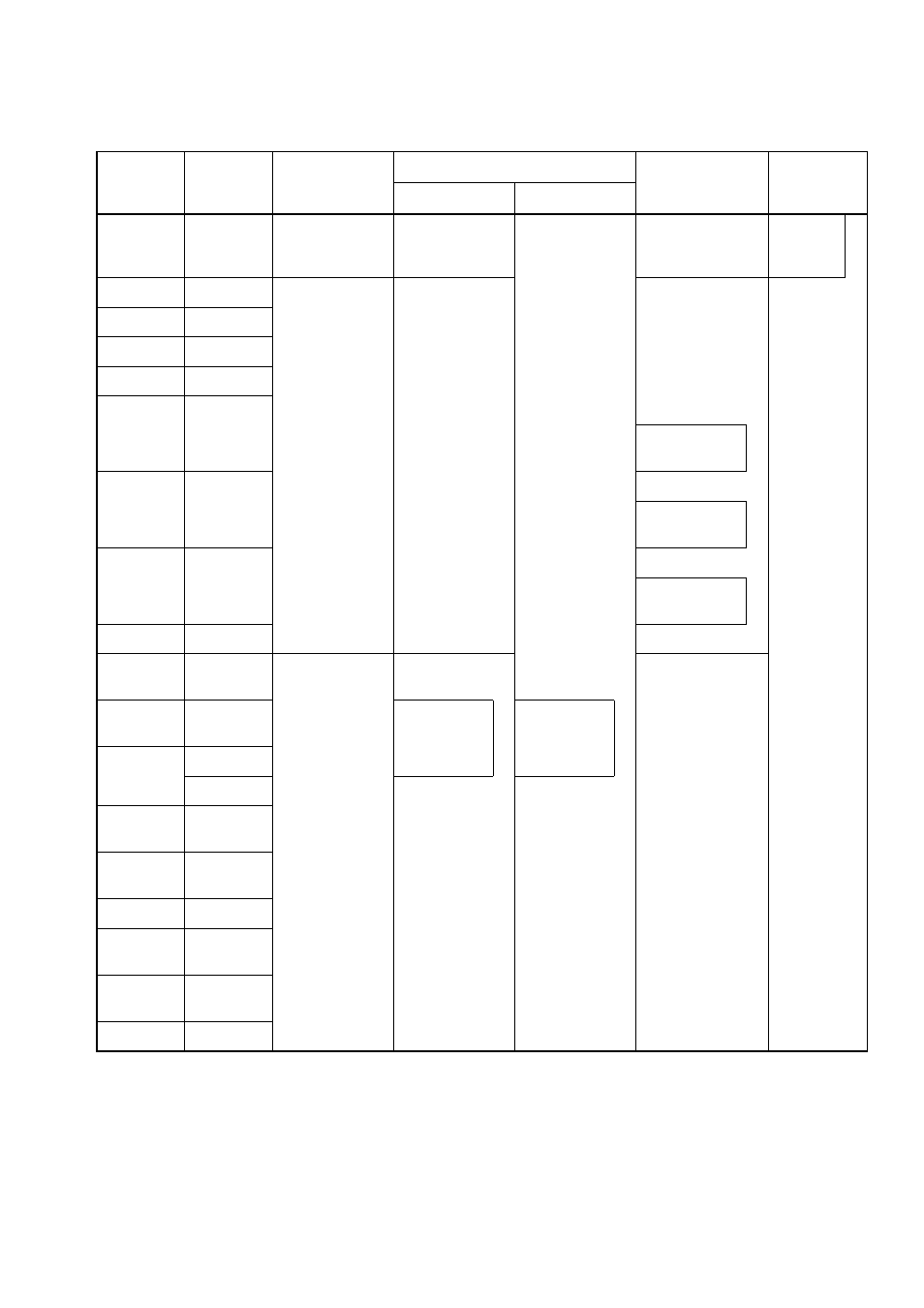
PA6
CLK
P: Previous
status retained
F: CLK output
P, F: Previous
status retained
Output Hi-Z/
Input fixed to 0
CLK Output
CLK
Output
PB0
RAS0
P: Previous
status retained
F: Previous
value retained
Executed when
DRAM pin is
set.
P: Previous
status retained
F: Previous
value retained
During refresh
(*1)
P: Previous
status retained
F: Previous value
retained
Operation during
DRAM terminal
setting
Output Hi-Z/
Input
allowed for
all pins
PB1
CS0L
PB2
CS0H
PB3
DW0X
PB4
RAS1
EOP2
Previous
value retained
PB5
CS1L
DREQ2
Previous
value retained
PB6
CS1H
DACK2
Previous
value retained
PB7
DW1X
AN0 to
AN3
AN0-3
Previous status
retained
Previous status
retained
PE0 to
PE2
INT0-INT2
Input
possible
Input
possible
PE3
INT3
SC2
Previous status
retained
PE4 to
PE5
DREQ0-
DREQ1
PE6 to
PE7
DACK0-
DACK1
PF0
SI0, TRG0
PF1
SO0,
TRG1
PF2
SC0,
OCPA3
PF3
SI1, TRG2
Table C-2 Pin Status for 16-bit External Bus Length and 2CA1WR Mode (Continued)
Pin name
Function
During sleep
During stop
Bus release
(BGRNT)
Reset time
HIZX=0
HIZX=1
- XG Series P3NK-4452-01ENZD (614 pages)
- FPCAC14C (1 page)
- MCJ3230SS (161 pages)
- MBA3073NC (138 pages)
- T5140 (76 pages)
- T5140 (102 pages)
- MAM3367MC/MP (152 pages)
- MPC3045AH (185 pages)
- MB2142-02 (23 pages)
- MB15F86UL (6 pages)
- MHS2030AT (40 pages)
- MHW2100BS (296 pages)
- MHK2060AT (227 pages)
- Disk Drives MHK2060AT (227 pages)
- MCM3064SS (170 pages)
- Mainboard D1561 (45 pages)
- MHC2040AT (219 pages)
- D1961 (45 pages)
- DISK DRIVES MHM2100AT (231 pages)
- MHR2010AT (250 pages)
- MHZ2120BJ (320 pages)
- MCE3064AP (175 pages)
- LQFP-64P (16 pages)
- Solaris PCI GigabitEthernet 3.0 (115 pages)
- MAY2036RC (94 pages)
- MAB3091 (142 pages)
- MPE3XXXAT (191 pages)
- MHV2040AH (40 pages)
- MHW2040AC (278 pages)
- ETERNUSmgr P2X0-0202-01EN (64 pages)
- VSS Hardware Provider 2.1 (134 pages)
- MAG3182FC (61 pages)
- MAU3147NC/NP (130 pages)
- MAX3147RC (94 pages)
- MHV2160BT (296 pages)
- MHV2040AT (280 pages)
- MAW3300NC/NP (130 pages)
- DeskPower E623 (50 pages)
- MAG3182LC (133 pages)
- OPTICAL DISK DRIVES MDG3064UB (42 pages)
- MHF2021AT (225 pages)
- MHR2040AT (40 pages)
- Single Drive FTM7926FB (1 page)
- PG-FCS103 (98 pages)
- MAS3735FC (114 pages)