FUJITSU MB91F109 FR30 User Manual
Page 138
114
CHAPTER 4 BUS INTERFACE
■
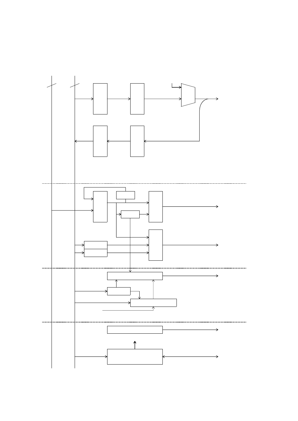
Block Diagram of the Bus Interface
Figure 4.1.2 shows a block diagram of the bus interface
Figure 4.1-2 Bus Interface Block Diagram
32
32
A-OUT
EXTERNAL
DATA BUS
MUX
write
buffer
switch
read buffer
switch
DATA BLOCK
ADDRESS BLOCK
+1or+2
EXTERNAL
ADDRESS BUS
inpage
address buffer
shifter
ASR
CS0X-CS5X
AMR
comparator
DRAM control
RAS0,RAS1
CS0L,CS1L
CS0H,CS1H
underflow
DW0X,DW1X
DMCR
refresh
counter
from TBT
RDX
WR0X,WR1X
BRQ
registers
BGRNTX
&
CLK
control
RDY
ADDRESS BUS
DATA BUS
External pin control block
Control of all blocks
See also other documents in the category FUJITSU Hardware:
- XG Series P3NK-4452-01ENZD (614 pages)
- FPCAC14C (1 page)
- MCJ3230SS (161 pages)
- MBA3073NC (138 pages)
- T5140 (76 pages)
- T5140 (102 pages)
- MAM3367MC/MP (152 pages)
- MPC3045AH (185 pages)
- MB2142-02 (23 pages)
- MB15F86UL (6 pages)
- MHS2030AT (40 pages)
- MHW2100BS (296 pages)
- MHK2060AT (227 pages)
- Disk Drives MHK2060AT (227 pages)
- MCM3064SS (170 pages)
- Mainboard D1561 (45 pages)
- MHC2040AT (219 pages)
- D1961 (45 pages)
- DISK DRIVES MHM2100AT (231 pages)
- MHR2010AT (250 pages)
- MHZ2120BJ (320 pages)
- MCE3064AP (175 pages)
- LQFP-64P (16 pages)
- Solaris PCI GigabitEthernet 3.0 (115 pages)
- MAY2036RC (94 pages)
- MAB3091 (142 pages)
- MPE3XXXAT (191 pages)
- MHV2040AH (40 pages)
- MHW2040AC (278 pages)
- ETERNUSmgr P2X0-0202-01EN (64 pages)
- VSS Hardware Provider 2.1 (134 pages)
- MAG3182FC (61 pages)
- MAU3147NC/NP (130 pages)
- MAX3147RC (94 pages)
- MHV2160BT (296 pages)
- MHV2040AT (280 pages)
- MAW3300NC/NP (130 pages)
- DeskPower E623 (50 pages)
- MAG3182LC (133 pages)
- OPTICAL DISK DRIVES MDG3064UB (42 pages)
- MHF2021AT (225 pages)
- MHR2040AT (40 pages)
- Single Drive FTM7926FB (1 page)
- PG-FCS103 (98 pages)
- MAS3735FC (114 pages)