18 internal clock multiplication (clock doubler) – FUJITSU MB91F109 FR30 User Manual
Page 218
194
CHAPTER 4 BUS INTERFACE
4.18 Internal Clock Multiplication (Clock Doubler)
The MB91F109 has a clock multiplication circuit with which the inside of the CPU
operates at a frequency one or two times that of the bus interface. The bus interface
operates synchronously with the CLK output pin regardless of which clock is chosen.
When an external access request is generated from the CPU, access to the outside
starts and waits for the CLK output to rise.
This device type is not provided with this function.
■
How to Choose Clocks
For details on choosing the 1X and 2X clocks, see Section 3.14, "Clock Doubler Function."
A chosen clock can be optionally changed during chip operation. When the clock is being
switched, the bus operation is temporarily suppressed. When the chip is reset, the 1X clock is
selected automatically.
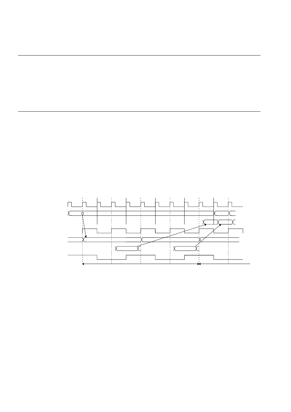
Figure 4.18-1 shows example of a 2X clock timing chart. Figure 4.18-2 shows an example of a
1X clock timing chart.
Figure 4.18-1 Example of Timing Chart for 2X Clock (BW-16bit, Access-Word Read)
Internal clock
Internal instruction
Internal instruction
CLK output
External address bus
External data bus
External RDX
Prefetch
External fetch (instruction fetch)
address
data
N
N
D
N + 1
N + 4
D + 2
D
D + 2
N + 2