Baud rates and clock frequencies, Baud rates and clock frequencies –6 – Altera RapidIO MegaCore Function User Manual
Page 52
4–6
Chapter 4: Functional Description
Clocking and Reset Structure
RapidIO MegaCore Function
August 2014
Altera Corporation
User Guide
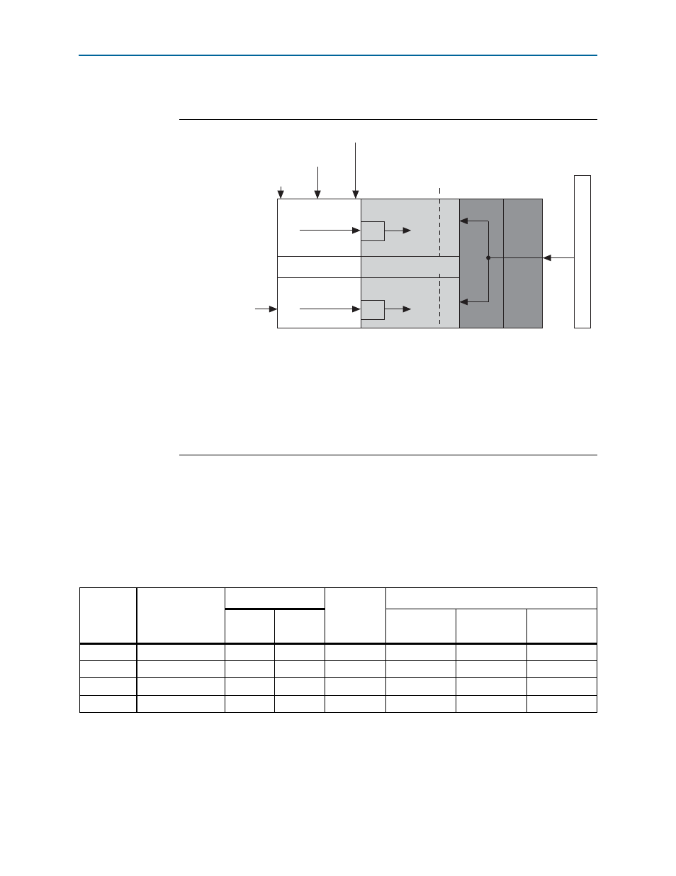
is a block diagram of the clock structure of the RapidIO IP core.
Baud Rates and Clock Frequencies
The RapidIO specification specifies baud rates of 1.25, 2.5, 3.125, and 5.0 Gbaud.
Table 4–2
and
Table 4–3
show the relationship between baud rates, transceiver clock
rates, and internal clock rates. For information about device family support for
different RapidIO variations, refer to
and
Figure 4–2. Clock Domains in RapidIO IP Core
Notes to
:
(1) Clock descriptions:
phy_mgmt_clk
PHY IP core management clock (Arria V, Cyclone V, Stratix V devices only)
reconfig_clk_chN
Arria 10 transceiver dynamic reconfiguration interface clock (Arria 10 devices only)
rxclk
Receiver internal global clock (recovered clock)
rxgxbclk
Receiver transceiver clock
txclk
Transmitter internal global clock
tx_bonding_clocks_chN
Transmitter transceiver clock
(2) The Avalon system clock is called sysclk.
Logical
Layer
Transport
Layer
clk
(reference clock)
Physical Layer Registers
Clock Domain
Boundary
Receiver
Transceiver
Transmitter
Transceiver
rxclk
rxgxbclk
txclk
Avalon
system
clock
(2)
S
y
s
t
e
m
I
n
t
e
r
c
o
n
n
e
c
t
phy_mgmt_clk
(Arria V, Cyclone V, Stratix V only)
Logical
Layer
Transport
Layer
clk
(reference clock)
Physical Layer Registers
Clock Domain
Boundary
Receiver
Transceiver
Transmitter
Transceiver
rxclk
rxgxbclk
tx_bonding_clocks_chN
(Arria 10 only)
txclk
Avalon
system
clock
(2)
S
y
s
t
e
m
I
n
t
e
r
c
o
n
n
e
c
t
phy_mgmt_clk
(Arria V, Cyclone V, Stratix V only)
reconfig_clk_chN
(Arria 10 only)
Table 4–2. Clock Frequencies for 1x and 2x RapidIO IP Core Variations
Baud Rate
(Gbaud)
Default reference
clock frequency
(1)
,
(2)
(MHz)
rxgxbclk
txclk, rxclk
(MHz)
Avalon system clock (sysclk)
1x
2x
Minimum
(MHz)
Typical
(MHz)
Maximum
(3)
(MHz)
1.25
62.5 62.5
31.25
31.25
15.625
31.25
46.875
2.5
125 125
62.5
62.5
31.25
62.5 93.75
3.125
156.25
156.25
78.125
78.125
39.065
78.125
117.19
5.0
250
250
125
125.0
62.50
125.0
187.50
Notes to
Table 4–2
:
(1) For information about the allowed reference clock frequencies, refer to
.
(2) The reference clock is called clk.
(3) The maximum system clock frequency might be limited by the achievable f
MAX
and can vary based on the family and speed grade.