Heading1 - dffn, Heading2 - negative clock edge d-type register, Figure - figure 2-7: logic symbol – Achronix Speedster22i User Macro Guide User Manual
Page 79: Heading2 - pins, Table - table 2-21: pin descriptions, Heading2 - parameters, Table - table 2-22: parameters, Heading3 - init, Table - table 2-23: function table, Dffn
Registers
DFFN
Speedster22i Macro Cell Library
PAGE 63
DFFN
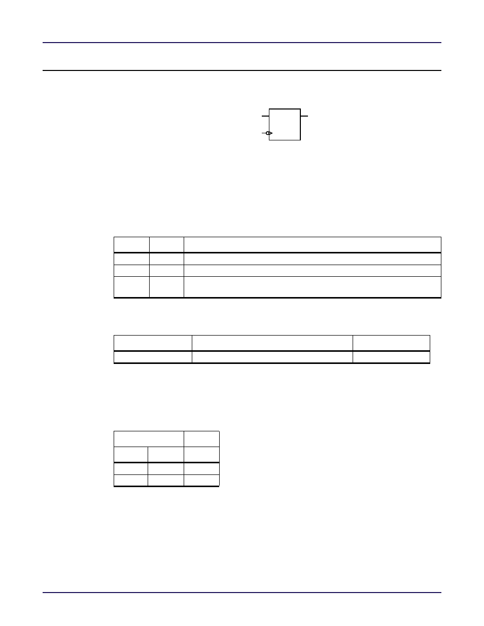
Negative Clock Edge D-Type Register
d
ckn
DFFN
q
Figure 2-7: Logic Symbol
DFFN is a single D‐type register with data input (d) and clock (ckn) inputs and data (q)
output. The data output is set to the value on the data input upon the next falling edge of the
clock.
Pins
Table 2-21: Pin Descriptions
Name
Type
Description
d
Data input.
ckn
Negative-edge clock input.
q
Data output. The value present on the data input is transferred to the q out-
put upon the falling edge of the clock.
Parameters
Table 2-22: Parameters
Parameter
Defined Values
Default Value
init
1’b0
init
The init parameter defines the initial value of the output of the DFFN register. This is the
value the register takes upon the initial application of power to the FPGA. The default value
of the init parameter is 1’b0.
Table 2-23: Function Table
Inputs
Output
d
ck
q
input
input
output
1’b0, 1’b1
0
0
1
1