Chaptertitle - chapter 6 – memories, Heading1 - bram80k, Heading2 - 80k-bit dual-port memory – Achronix Speedster22i User Macro Guide User Manual
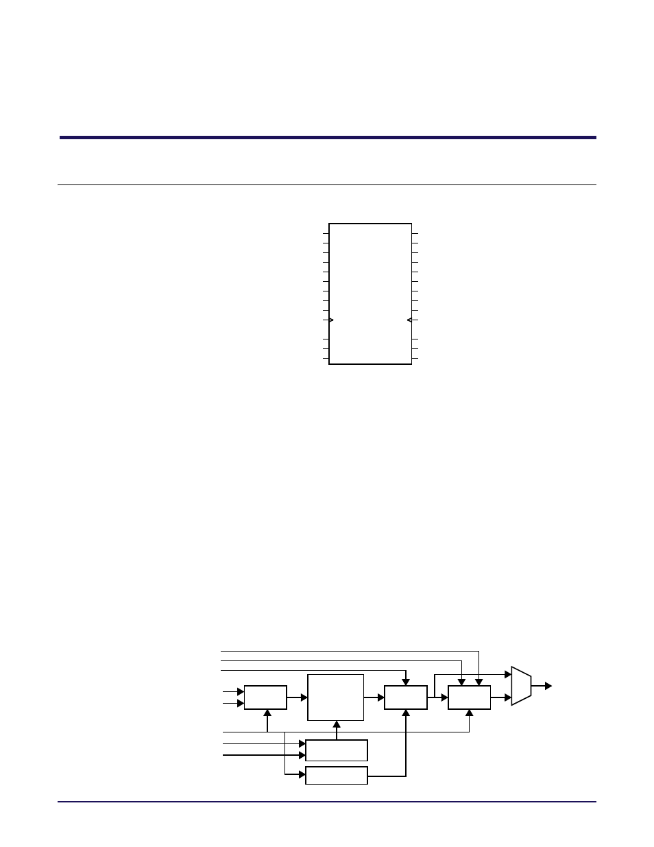
Page 106: Figure - figure 6-1: logic symbol, Chapter 6 – “memories, Bram80k
Speedster22i Macro Cell Library
PAGE 89
Chapter 6 – Memories
BRAM80K
80k-bit Dual-Port Memory
BRAM80K
addrb[15:0]
dinb[31:0]
peb
clkb
doutb[31:0]
addra[15:0]
dina[31:0]
wea[3:0]
pea
clka
douta[31:0]
dinpa[3:0]
dinpxa[3:0]
rstlatcha
rstrega
outregcea
doutpa[3:0]
doutpxa[3:0]
dinpb[3:0]
dinpxb[3:0]
web[3:0]
rstlatchb
rstregb
outregceb
doutpb[3:0]
doutpxb[3:0]
Figure 6-1: Logic Symbol
The block RAM (BRAM80K) implements a 80k‐bit dual‐ported memory block where each port
can be independently configured with respect to size and function. The BRAM80K can be
configured as a single‐port (1 r/w port), dual‐port (two r/w ports with independent clocks), or
ROM memory. Each memory can be configured as a 2kx40, 2kx36, 2kx32, 4kx20, 4kx18, 4kx16,
8kx10, 8kx9, 8kx8, 16kx5, 16kx4, 32kx2, or 64kx1. The read and write operations are both
synchronous. For higher performance operation, an addition output register can be enabled.
Enabling the output register will require an additional cycle of read latency. Write Enable
(wea/web) controls provide 10‐bit enable control for port widths of 10, 20 or 40 bit. The initial
value of the memory contents may be specified by the user from either parameters or a
memory initialization file. The initial/reset values of the output registers may also be specified
by the user. The porta_write_mode/portb_write_mode parameters define the behavior of the
output data port during a write operation. When porta_write_mode/portb_write_mode is set
to write_first, the douta/doutb is set to the value being written on the dina/dinb port during a
write operation. Setting porta_write_mode/portb_write_mode to no_change keeps the douta/
doutb port unchanged during a write operation to porta/portb. Conflict arises when the same
memory cell is accessed by both ports within a narrow window and one or both ports are
writing to memory. If this condition occurs, the contents of the memory for the colliding
address will be undefined, but no damage will occur to the Speedster FPGA:
Figure 6-2: BRAM80K Block Diagram (Per Port)
Memory
Register
Control
Latch
Register
Delay
ck
addr
din, dinp, dinpx
pe
we
rstlatch
rstreg
dout
outregce
doutp
doutpx