Heading1 - bram80keccfifo, Figure - figure 6-27: logic symbol, Figure - figure 6-28: bram80keccfifo block diagram – Achronix Speedster22i User Macro Guide User Manual
Page 170: Bram80keccfifo
Memories
BRAM80KECCFIFO
Speedster22i Macro Cell Library
PAGE 153
BRAM80KECCFIFO
80k-bit FIFO Memory with Error Correction
BRAM80KECCFIFO
dout[31:0]
doutp[3:0]
full
read_err
sbit_error
din[31:0]
dinp[3:0]
wrrst
rdrst
outregce
dinpx[3:0]
wren
rden
rstreg
doutpx[3:0]
empty
almost_empty
almost_full
write_err
dbit_error
wrclk
rdclk
rdaddrecc[10:0]
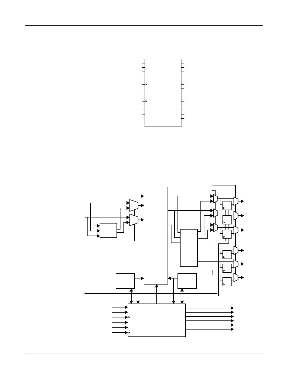
Figure 6-27: Logic Symbol
The BRAM80KECCFIFO implements a 2k deep, 32‐bit wide FIFO memory block utilizing the
embedded BRAM80K blocks with dedicated pointer and flag circuitry. The
BRAM80KECCFIFO has 2k locations of 32‐bit data. The read and write clocks may be either
synchronous or asynchronous with respect to each other. If the user read and write clocks are
the same clock, the user may set the sync_mode to 1’b1 to enable faster and synchronous
generation of the status flag outputs.
Figure 6-28: BRAM80KECCFIFO Block Diagram
32-bit
ECC
Encoder
2kx40
Dual-Port
Memory
din[31:0]
outregce
rstreg
dinp[3:0]
dinpx[3:0]
d q
32-bit
ECC
Decoder
d q
d q
d q
din
dinp
dinpx
dout
doutp
doutpx
sbit_error
dbit_error
rdaddrecc
d q
dbit_error
sbit_error
dout
doutp
doutpx
waddr raddr
d q
[10:0]
encoder_enable
decoder_enable
en_out_reg
[31:0]
[3:0]
[3:0]
Write
Pointer
Logic
Read
Pointer
Logic
Memory Control /
Flag Generation
Logic
full
empty
almost_full
almost_empty
write_err
read_err
wren
wrrst
wrclk
rdrst
rdclk
rden